- 您現(xiàn)在的位置:買賣IC網(wǎng) > PDF目錄383961 > TMX320DM647ZUT900 (Texas Instruments, Inc.) Digital Media Processor PDF資料下載
參數(shù)資料
| 型號(hào): | TMX320DM647ZUT900 |
| 廠商: | Texas Instruments, Inc. |
| 英文描述: | Digital Media Processor |
| 中文描述: | 數(shù)字媒體處理器 |
| 文件頁(yè)數(shù): | 140/166頁(yè) |
| 文件大?。?/td> | 1341K |
| 代理商: | TMX320DM647ZUT900 |
第1頁(yè)第2頁(yè)第3頁(yè)第4頁(yè)第5頁(yè)第6頁(yè)第7頁(yè)第8頁(yè)第9頁(yè)第10頁(yè)第11頁(yè)第12頁(yè)第13頁(yè)第14頁(yè)第15頁(yè)第16頁(yè)第17頁(yè)第18頁(yè)第19頁(yè)第20頁(yè)第21頁(yè)第22頁(yè)第23頁(yè)第24頁(yè)第25頁(yè)第26頁(yè)第27頁(yè)第28頁(yè)第29頁(yè)第30頁(yè)第31頁(yè)第32頁(yè)第33頁(yè)第34頁(yè)第35頁(yè)第36頁(yè)第37頁(yè)第38頁(yè)第39頁(yè)第40頁(yè)第41頁(yè)第42頁(yè)第43頁(yè)第44頁(yè)第45頁(yè)第46頁(yè)第47頁(yè)第48頁(yè)第49頁(yè)第50頁(yè)第51頁(yè)第52頁(yè)第53頁(yè)第54頁(yè)第55頁(yè)第56頁(yè)第57頁(yè)第58頁(yè)第59頁(yè)第60頁(yè)第61頁(yè)第62頁(yè)第63頁(yè)第64頁(yè)第65頁(yè)第66頁(yè)第67頁(yè)第68頁(yè)第69頁(yè)第70頁(yè)第71頁(yè)第72頁(yè)第73頁(yè)第74頁(yè)第75頁(yè)第76頁(yè)第77頁(yè)第78頁(yè)第79頁(yè)第80頁(yè)第81頁(yè)第82頁(yè)第83頁(yè)第84頁(yè)第85頁(yè)第86頁(yè)第87頁(yè)第88頁(yè)第89頁(yè)第90頁(yè)第91頁(yè)第92頁(yè)第93頁(yè)第94頁(yè)第95頁(yè)第96頁(yè)第97頁(yè)第98頁(yè)第99頁(yè)第100頁(yè)第101頁(yè)第102頁(yè)第103頁(yè)第104頁(yè)第105頁(yè)第106頁(yè)第107頁(yè)第108頁(yè)第109頁(yè)第110頁(yè)第111頁(yè)第112頁(yè)第113頁(yè)第114頁(yè)第115頁(yè)第116頁(yè)第117頁(yè)第118頁(yè)第119頁(yè)第120頁(yè)第121頁(yè)第122頁(yè)第123頁(yè)第124頁(yè)第125頁(yè)第126頁(yè)第127頁(yè)第128頁(yè)第129頁(yè)第130頁(yè)第131頁(yè)第132頁(yè)第133頁(yè)第134頁(yè)第135頁(yè)第136頁(yè)第137頁(yè)第138頁(yè)第139頁(yè)當(dāng)前第140頁(yè)第141頁(yè)第142頁(yè)第143頁(yè)第144頁(yè)第145頁(yè)第146頁(yè)第147頁(yè)第148頁(yè)第149頁(yè)第150頁(yè)第151頁(yè)第152頁(yè)第153頁(yè)第154頁(yè)第155頁(yè)第156頁(yè)第157頁(yè)第158頁(yè)第159頁(yè)第160頁(yè)第161頁(yè)第162頁(yè)第163頁(yè)第164頁(yè)第165頁(yè)第166頁(yè)
www.ti.com
P
TMS320DM647/TMS320DM648
Digital Media Processor
SPRS372–MAY 2007
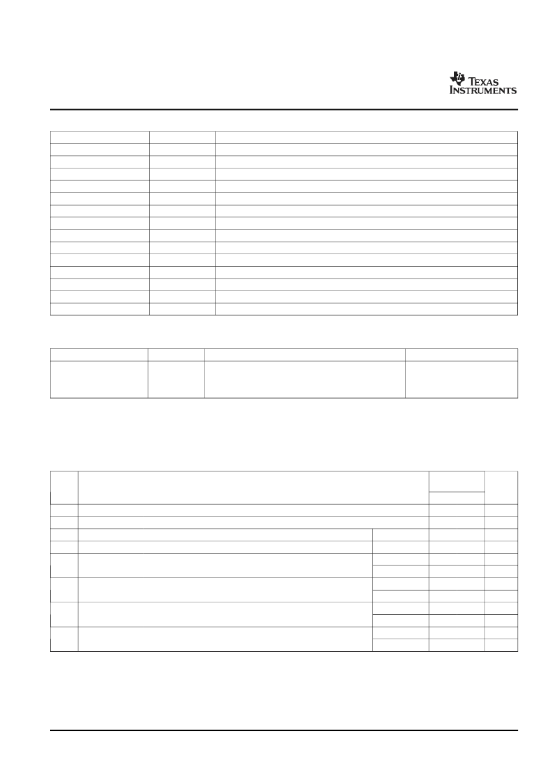
Table 6-59. McASP Control Registers (continued)
HEX ADDRESS RANGE
0x0204 021A
0x0204 0220
0x0204 0224-0x0204 027C
0x0204 0280
0x0204 0284
0x0204 0288
0x0204 028C
0x0204 0290
0x0204 0294
0x0204 0298
0x0204 029C
0x0204 02A0
0x0204 02A4
0x0204 02A8-0x0204 3FFF
ACRONYM
XBUF8
XBUF9
–
RBUF0
RBUF1
RBUF2
RBUF3
RBUF4
RBUF5
RBUF6
RBUF7
RBUF8
RBUF9
–
REGISTER NAME
Transmit Buffer for Serializer 8
Transmit Buffer for Serializer 9
Reserved
Receive Buffer for Serializer 0
Receive Buffer for Serializer 1
Receive Buffer for Serializer 2
Receive Buffer for Serializer 3
Receive Buffer for Serializer 4
Receive Buffer for Serializer 5
Receive Buffer for Serializer 6
Receive Buffer for Serializer 7
Receive Buffer for Serializer 8
Receive Buffer for Serializer 9
Reserved
Table 6-60. McASP Data Registers
HEX ADDRESS RANGE
ACRONYM
REGISTER NAME
COMMENTS
(Used when RSEL or XSEL
bits = 0 [these bits are located
in the RFMT or XFMT registers,
respectively].)
McASP receive buffers or McASP transmit buffers via the
Peripheral Data Bus.
01D0 1400 – 01D0 17FF
RBUF/XBUF0
6.17.1.3
McASP Electrical Data/Timing
6.17.1.3.1
Multichannel Audio Serial Port (McASP) Timing
Table 6-61. Timing Requirements for McASP (see
Figure 6-40
and
Figure 6-41
)
(1)
-720
-900
NO.
UNIT
MIN
MAX
1
2
3
4
t
c(AHCKRX)
t
w(AHCKRX)
t
c(CKRX)
t
w(CKRX)
Cycle time, AHCLKR/X
Pulse duration, AHCLKR/X high or low
Cycle time, ACLKR/X
Pulse duration, ACLKR/X high or low
20
10
33
ns
ns
ns
ns
ns
ns
ns
ns
ns
ns
ns
ns
ACLKR/X ext
ACLKR/X ext
ACLKR/X int
ACLKR/X ext
ACLKR/X int
ACLKR/X ext
ACLKR/X int
ACLKR/X ext
ACLKR/X int
ACLKR/X ext
16.5
5
5
5
5
5
5
5
5
5
t
su(FRX-CKRX)
Setup time, AFSR/X input valid before ACLKR/X latches data
6
t
h(CKRX-FRX)
Hold time, AFSR/X input valid after ACLKR/X latches data
7
t
su(AXR-CKRX)
Setup time, AXR input valid before ACLKR/X latches data
8
t
h(CKRX-AXR)
Hold time, AXR input valid after ACLKR/X latches data
(1)
ACLKX internal: ACLKXCTL.CLKXM=1, PDIR.ACLKX = 1
ACLKX external input: ACLKXCTL.CLKXM=0, PDIR.ACLKX=0
ACLKX external output: ACLKXCTL.CLKXM=0, PDIR.ACLKX=1
ACLKR internal: ACLKRCTL.CLKRM=1, PDIR.ACLKR = 1
ACLKR external input: ACLKRCTL.CLKRM=0, PDIR.ACLKR=0
ACLKR external output: ACLKRCTL.CLKRM=0, PDIR.ACLKR=1
Peripheral Information and Electrical Specifications
140
Submit Documentation Feedback
相關(guān)PDF資料 |
PDF描述 |
|---|---|
| TMX320DM648ZUT720 | Digital Media Processor |
| TMX320DM648ZUT900 | Digital Media Processor |
| TMS320LC31PQL | DIGITAL SIGNAL PROCESSORS |
| TMX320C6414TGLZ | FIXED-POINT DIGITAL SIGNAL PROCESSORS |
| TMX320C6415TGLZ | FIXED-POINT DIGITAL SIGNAL PROCESSORS |
相關(guān)代理商/技術(shù)參數(shù) |
參數(shù)描述 |
|---|---|
| TMX320DM648ACUT7 | 制造商:Texas Instruments 功能描述:- Trays |
| TMX320DM648ACUT9 | 制造商:Texas Instruments 功能描述:- Trays |
| TMX320DM648AZUT7 | 制造商:Texas Instruments 功能描述: |
| TMX320DM648CUT7 | 制造商:Texas Instruments 功能描述:- Trays |
| TMX320DM648ZUT7 | 功能描述:數(shù)字信號(hào)處理器和控制器 - DSP, DSC Dig Media Processor RoHS:否 制造商:Microchip Technology 核心:dsPIC 數(shù)據(jù)總線寬度:16 bit 程序存儲(chǔ)器大小:16 KB 數(shù)據(jù) RAM 大小:2 KB 最大時(shí)鐘頻率:40 MHz 可編程輸入/輸出端數(shù)量:35 定時(shí)器數(shù)量:3 設(shè)備每秒兆指令數(shù):50 MIPs 工作電源電壓:3.3 V 最大工作溫度:+ 85 C 封裝 / 箱體:TQFP-44 安裝風(fēng)格:SMD/SMT |
發(fā)布緊急采購(gòu),3分鐘左右您將得到回復(fù)。