- 您現(xiàn)在的位置:買賣IC網(wǎng) > PDF目錄385942 > TNETA1556 (Texas Instruments, Inc.) 155.52-Mbit/S Clock-Recovery Device(155.52-MBIT/S時(shí)鐘恢復(fù)裝置) PDF資料下載
參數(shù)資料
| 型號(hào): | TNETA1556 |
| 廠商: | Texas Instruments, Inc. |
| 英文描述: | 155.52-Mbit/S Clock-Recovery Device(155.52-MBIT/S時(shí)鐘恢復(fù)裝置) |
| 中文描述: | 155.52 - Mbit / s的時(shí)鐘恢復(fù)裝置(155.52 - Mbit / s的時(shí)鐘恢復(fù)裝置) |
| 文件頁(yè)數(shù): | 5/10頁(yè) |
| 文件大小: | 216K |
| 代理商: | TNETA1556 |
TNETA1556
155.52-MBIT/S CLOCK-RECOVERY DEVICE
SDNS015C – FEBRUARY 1994 – REVISED JUNE 1995
5
POST OFFICE BOX 655303
DALLAS, TEXAS 75265
APPLICATION INFORMATION
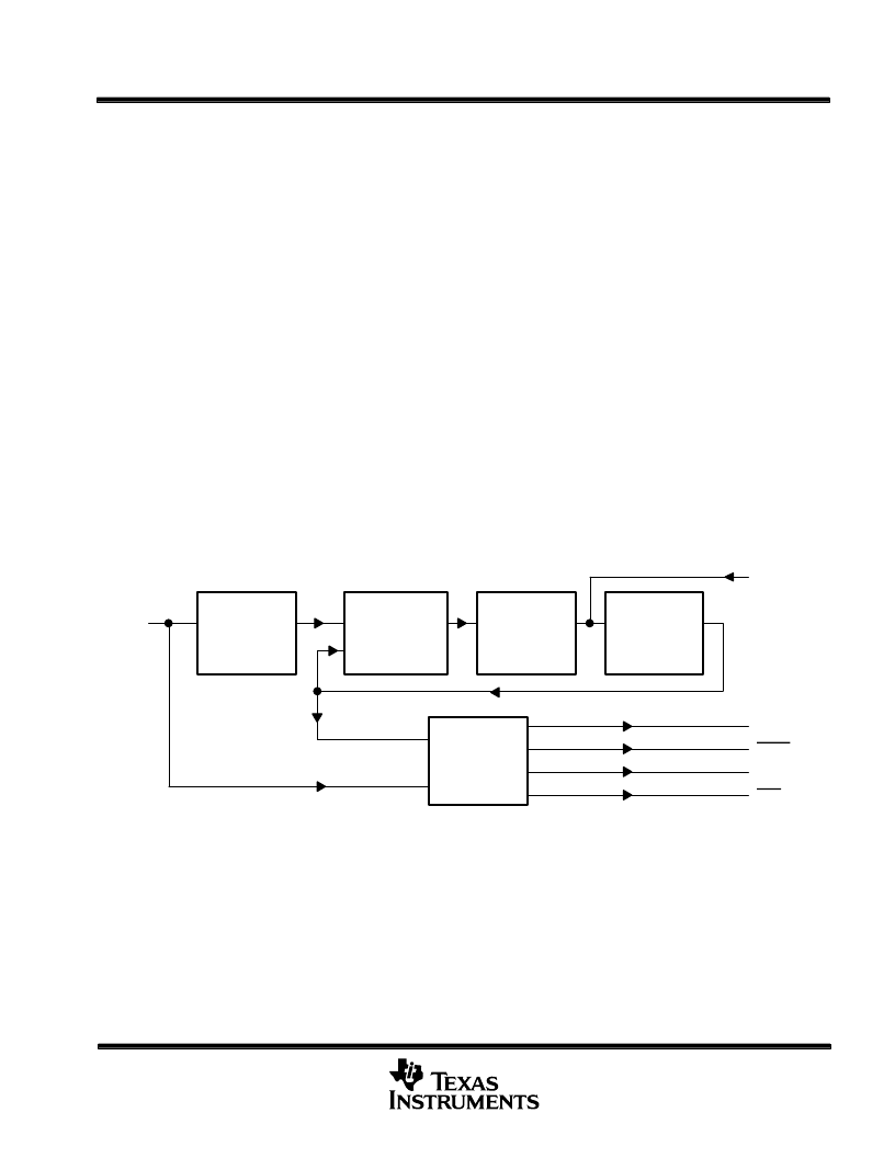
The TNETA1556 clock-recovery device provides clock recovery and data retiming on a nonreturn to zero (NRZ)
serial input data stream. The device uses an analog phase-lock loop (APLL) with an integrated
voltage-controlled oscillator (VCO) to recover the imbedded clock signal from incoming data. A loop-filter
capacitor is the only external component required for the proper operation of the device. The TNETA1556 is
designed for operation with a 155.52-Mbit/s serial data stream. This device has pseudo-ECL-compatible or
ECL-compatible inputs and ECL-compatible outputs and operates from a single 5-V supply. Pseudo-ECL levels
are ECL levels referenced to 5 V instead of ground.
Since the incoming 155.52-Mbit/s data stream does not contain a 155.52-MHz frequency component, a
transition detector, shown in the clock-recovery block diagram, is used as a frequency doubler to generate this
frequency. The output of the transition detector is passed to a phase/frequency detector where it is compared
to the output of the VCO. The phase/frequency detector is actually comprised of two circuits. One circuit provides
a coarse frequency-detection capability and a second provides a finer phase adjustment. The phase/frequency
detector compares the signal from the transition detector to the VCO output and generates signals to either
increase or decrease the VCO frequency depending upon whether the VCO frequency is less than or greater
than the frequency of the signal from the transition detector. The up/down pulses are sent to the charge
pump/loop filter for conversion to a bias voltage that sets the VCO output frequency.
The process of comparing the input signal frequency and the VCO output frequency is continuous and
eventually results in the VCO output frequency equaling the frequency of the input signal. It also allows the VCO
output to react to changes in the input signal due to jitter. The recovered clock output is sent from the VCO to
the retiming circuit where the input data is retimed to the recovered clock. The retiming circuit centers the output
clock in the middle of the output data.
clock-recovery block diagram
DOUT
DOUT
CLK
CLK
Retiming
Circuit
Transition
Detector
Phase/Frequency
Detector
Charge Pump/
Loop Filter
Voltage-
Controlled
Oscillator
Recovered
Clock
DIN
CPLL
performance measurements
Measuring the performance of a clock-recovery circuit involves determining how well the circuit operates in the
presence of jitter. Jitter is defined as the short-term variations of a digital signals significant instants from their
ideal positions in time.
For testing purposes, jitter is usually generated by modulating a digital data sequence
with a sinusoidal waveform of a known frequency. This results in a digital data stream where the widths of the
individual data pulses varies with time. The amount of pulse width variation can be changed by altering the
frequency and amplitude of the modulating signal, which changes the amount of jitter in the data stream. The
following paragraphs describe the test results obtained from the TNETA1556 for various performance
measurements.
Bellcore technical reference TR-TSY-000499 Issue 3, December 1989, page 7-1.
P
相關(guān)PDF資料 |
PDF描述 |
|---|---|
| TNETA1560 | ATM Segmentation and Reassembly Device with SBUS Host Interface(ATM 分段和重設(shè)裝置帶SBUS主機(jī)接口) |
| TNETA1561 | ATM Segmentation and Reassembly Device with PCI Host Interface(ATM 分段和重設(shè)裝置帶SBUS主機(jī)接口) |
| TNETA1600 | SONET/SDH ATM Receiver/Transmitter for 622.08-Mit/s or 155.52-Mbit/s Operation(SONET/SDH ATM接收器/傳送器) |
| TNETA1610 | STS-12c/STM-4 Receiver/Transmitter with Clock Recovery/Generation(STS-12C/STM-4接收/傳送器) |
| TNETA1611 | STS-12c/STM-4 Receiver/Transimitter(STS-12C/STM-4接收/傳送器) |
相關(guān)代理商/技術(shù)參數(shù) |
參數(shù)描述 |
|---|---|
| TNETA1560MFP | 制造商:Rochester Electronics LLC 功能描述: 制造商:Texas Instruments 功能描述: |
| TNETA1560PGC | 制造商:Rochester Electronics LLC 功能描述:- Bulk |
| TNETA1561PGC | 制造商:Rochester Electronics LLC 功能描述:- Bulk |
| TNETA1570 | 制造商:TI 制造商全稱:Texas Instruments 功能描述:ATM SEGMENTATION AND REASSEMBLY DEVICE WITH INTEGRATED 64-BIT PCI-HOST INTERFACE |
| TNETA1570MFP | 制造商:未知廠家 制造商全稱:未知廠家 功能描述:ATM/SONET Segmentation and Reassembly Circuit |
發(fā)布緊急采購(gòu),3分鐘左右您將得到回復(fù)。