- 您現(xiàn)在的位置:買賣IC網 > PDF目錄98274 > TPA5050RSARG4 (TEXAS INSTRUMENTS INC) SPECIALTY CONSUMER CIRCUIT, PQCC16 PDF資料下載
參數資料
| 型號: | TPA5050RSARG4 |
| 廠商: | TEXAS INSTRUMENTS INC |
| 元件分類: | 消費家電 |
| 英文描述: | SPECIALTY CONSUMER CIRCUIT, PQCC16 |
| 封裝: | 4 X 4 MM, GREEN, PLASTIC, QFN-16 |
| 文件頁數: | 4/21頁 |
| 文件大小: | 784K |
| 代理商: | TPA5050RSARG4 |

www.ti.com
APPLICATION EXAMPLES
Single Byte Write
D2
Start
ACK
01
ACK
C0
ACK
Stop
TPA5050 Addressand
Write
Register Address
Data
Multiple Byte Write
D2
Start
ACK
01
00
0F
ACK
Stop
TPA5050 Addressand
Write
Register Address
(ControlRegister)
Data
(RightDelayUpperBits)
ACK
FF
ACK
Data
(ControlRegister)
Data
(RightDelayLowerBits)
10
ACK
00
ACK
Data
(LeftDelayUpperBits)
Data
(RJPacket=0Bits)
ACK
01
ACK
Data
(FrameDelay)
Data
(CompleteUpdate)
Data
(LeftDelayLowerBits)
Combination Single Byte Write and Sequential Write
D2
Start
ACK
01
ACK
01
ACK
Stop
TPA5050 Addressand
Write
Register Address
(ControlRegister)
Data
(ControlRegister)
D2
Start
ACK
06
ACK
91
ACK
10
TPA5050 Addressand
Write
Register Address
(FrameDelay)
Data
(FrameDelay)
01
ACK
Data
(RJPacket=16Bits)
Stop
Data
(CompleteUpdate)
ACK
SLOS492B – MAY 2006 – REVISED MAY 2007
Table 7. Complete Update Registers (0x08)(1)
D7–D1
D0
FUNCTION
X
0
No data from the register settings is passed to the delay block.
X
1
Stream type, right/left delay or frame delay, and packet length is passed to the delay functional block.
(1)
Default values are in bold.
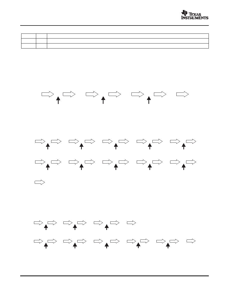
The following are some examples of I2C commands used to read or write to the TPA5050. For all conditions,
assume the address of the TPA5050 is set to 001.
In this example, the TPA5050 is set to mute both left and right channels, and to operate in I2S mode.
In this example, the TPA5050 is set to make both the left and right channels active, operate in I2S mode, delay
the right channel by 4095 samples, and delay the left channel by 4096 samples. This is a sequential write, so all
registers must have data written to them.
In this example, the TPA5050 is set to operate in the Right Justified mode, with a packet length of 16 bits. The
device is to delay the audio signal by 40 ms using the Frame Delay function. Assume the audio sample rate (fs)
= 48 kHz, and the Frame rate = 50 Hz. This is a combination of single writes and a sequential write. Since the
Right Justified mode is set in the Control Register, and the Frame Delay is set in register 0x06, the data in
registers 0x02–0x05 can be ignored.
Note that in every circumstance where a delay was written into the memory of the TPA5050, a 1 must be written
to the Complete Data register for the change to take effect. This does not apply to muting, which occurs in the
Control register.
12
相關PDF資料 |
PDF描述 |
|---|---|
| TPA5050RSAR | SPECIALTY CONSUMER CIRCUIT, PQCC16 |
| TPA5050RSATG4 | SPECIALTY CONSUMER CIRCUIT, PQCC16 |
| TPA5050RSAT | SPECIALTY CONSUMER CIRCUIT, PQCC16 |
| TPA5051RSARG4 | SPECIALTY CONSUMER CIRCUIT, PQCC16 |
| TPA5051RSAR | SPECIALTY CONSUMER CIRCUIT, PQCC16 |
相關代理商/技術參數 |
參數描述 |
|---|---|
| TPA5050RSAT | 功能描述:音頻 DSP St Dig Aud Delay Proc RoHS:否 制造商:Texas Instruments 工作電源電壓: 電源電流: 工作溫度范圍: 安裝風格: 封裝 / 箱體: 封裝:Tube |
| TPA5050RSATG4 | 功能描述:音頻 DSP St Dig Aud Delay Proc RoHS:否 制造商:Texas Instruments 工作電源電壓: 電源電流: 工作溫度范圍: 安裝風格: 封裝 / 箱體: 封裝:Tube |
| TPA5051 | 制造商:TI 制造商全稱:Texas Instruments 功能描述:FOUR CHANNEL DIGITAL AUDIO LIP-SYNC DELAY WITH I2C CONTROL |
| TPA5051_07 | 制造商:TI 制造商全稱:Texas Instruments 功能描述:FOUR CHANNEL DIGITAL AUDIO LIP-SYNC DELAY WITH I2C CONTROL |
| TPA5051EVM | 功能描述:音頻 IC 開發(fā)工具 AUD DELAY DEVICE RoHS:否 制造商:Texas Instruments 產品:Evaluation Kits 類型:Audio Amplifiers 工具用于評估:TAS5614L 工作電源電壓:12 V to 38 V |
發(fā)布緊急采購,3分鐘左右您將得到回復。