- 您現(xiàn)在的位置:買賣IC網(wǎng) > PDF目錄98282 > TPS51211DSCR (TEXAS INSTRUMENTS INC) SWITCHING CONTROLLER, 314 kHz SWITCHING FREQ-MAX, PDSO10 PDF資料下載
參數(shù)資料
| 型號(hào): | TPS51211DSCR |
| 廠商: | TEXAS INSTRUMENTS INC |
| 元件分類: | 穩(wěn)壓器 |
| 英文描述: | SWITCHING CONTROLLER, 314 kHz SWITCHING FREQ-MAX, PDSO10 |
| 封裝: | PLASTIC, SON-10 |
| 文件頁(yè)數(shù): | 9/26頁(yè) |
| 文件大?。?/td> | 674K |
| 代理商: | TPS51211DSCR |
第1頁(yè)第2頁(yè)第3頁(yè)第4頁(yè)第5頁(yè)第6頁(yè)第7頁(yè)第8頁(yè)當(dāng)前第9頁(yè)第10頁(yè)第11頁(yè)第12頁(yè)第13頁(yè)第14頁(yè)第15頁(yè)第16頁(yè)第17頁(yè)第18頁(yè)第19頁(yè)第20頁(yè)第21頁(yè)第22頁(yè)第23頁(yè)第24頁(yè)第25頁(yè)第26頁(yè)
IND(ripple)
OUT
I
ESR
V
0.7
2
R1
R2
0.7
-
÷
÷
è
=
UDG-10162
TPS51211
DRVL
4
VIN
1 mF
VFB
V5IN
V
OUT
2
TRIP
5
TST
# 2
# 1
# 3
5
6
Thermal Pad
GND
TPS51211
www.ti.com
SLUSAA7 – NOVEMBER 2010
3. Determine the value of R1 and R2.
The output voltage is programmed by the voltage-divider resistor, R1 and R2, shown in Figure 14. R1 is
connected between the VFB pin and the output, and R2 is connected between the VFB pin and GND. Typical
designs begin with the selection of an R2 value between 10 k
and 20 k. Determine R1 using Equation 9.
(9)
LAYOUT CONSIDERATIONS
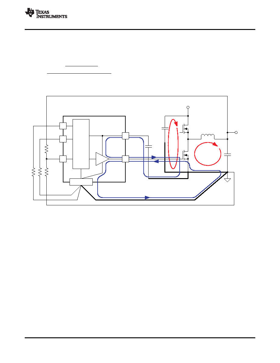
Figure 16. Ground System of DC/DC Converter Using the TPS51211
Certain points must be considered before starting a layout work using the TPS51211.
Inductor, VIN capacitor(s), VOUT capacitor(s) and MOSFETs are the power components and should be placed
on one side of the PCB (solder side). Other small signal components should be placed on another side
(component side). At least one inner plane should be inserted, connected to ground, in order to shield and
isolate the small signal traces from noisy power lines.
All sensitive analog traces and components such as VFB, PGOOD, TRIP and TST should be placed away
from high-voltage switching nodes such as SW, DRVL, DRVH or VBST to avoid coupling. Use internal
layer(s) as ground plane(s) and shield feedback trace from power traces and components.
The DC/DC converter has several high-current loops. The area of these loops should be minimized in order to
suppress generating switching noise.
–
The most important loop to minimize the area of is the path from the VIN capacitor(s) through the high and
low-side MOSFETs, and back to the capacitor(s) through ground. Connect the negative node of the VIN
capacitor(s) and the source of the low-side MOSFET at ground as close as possible. (Refer to loop #1 of
–
The second important loop is the path from the low-side MOSFET through inductor and VOUT capacitor(s),
and back to source of the low-side MOSFET through ground. Connect source of the low-side MOSFET
and negative node of VOUT capacitor(s) at ground as close as possible. (Refer to loop #2 of Figure 16)
–
The third important loop is of gate driving system for the low-side MOSFET. To turn on the low-side
MOSFET, high current flows from V5IN capacitor through gate driver and the low-side MOSFET, and back
to negative node of the capacitor through ground. To turn off the low-side MOSFET, high current flows
from gate of the low-side MOSFET through the gate driver and GND pad of the device, and back to
Copyright 2010, Texas Instruments Incorporated
17
相關(guān)PDF資料 |
PDF描述 |
|---|---|
| TPS51220ARTVR | DUAL SWITCHING CONTROLLER, 333 kHz SWITCHING FREQ-MAX, PQCC32 |
| TPS51221RTVRG4 | DUAL SWITCHING CONTROLLER, 333 kHz SWITCHING FREQ-MAX, PQCC32 |
| TPS51315RGFR | SWITCHING REGULATOR, 1000 kHz SWITCHING FREQ-MAX, PQCC40 |
| TPS51315RGFT | SWITCHING REGULATOR, 1000 kHz SWITCHING FREQ-MAX, PQCC40 |
| TPS51317RGBT | SWITCHING REGULATOR, 1500 kHz SWITCHING FREQ-MAX, PQCC20 |
相關(guān)代理商/技術(shù)參數(shù) |
參數(shù)描述 |
|---|---|
| TPS51211DSCT | 功能描述:DC/DC 開關(guān)控制器 Hi-Perf,Single Synch Step-Down Controller RoHS:否 制造商:Texas Instruments 輸入電壓:6 V to 100 V 開關(guān)頻率: 輸出電壓:1.215 V to 80 V 輸出電流:3.5 A 輸出端數(shù)量:1 最大工作溫度:+ 125 C 安裝風(fēng)格: 封裝 / 箱體:CPAK |
| TPS51212DSCR | 制造商:Texas Instruments 功能描述:LOW COST SINGLE PHASE DC/DC CONTROLLER |
| TPS51216 | 制造商:TI 制造商全稱:Texas Instruments 功能描述:Complete DDR2, DDR3 and DDR3L Memory Power Solution Synchronous Buck Controller, 2-A LDO, Buffered Reference |
| TPS51216MRUKREP | 功能描述:D-CAP? Controller, DDR Voltage Regulator IC 2 Output 20-WQFN (3x3) 制造商:texas instruments 系列:D-CAP?? 包裝:剪切帶(CT) 零件狀態(tài):有效 應(yīng)用:控制器,DDR 電壓 - 輸入:4.5 V ~ 5.5 V 輸出數(shù):2 電壓 - 輸出:0.7 V ~ 1.8 V 工作溫度:-55°C ~ 125°C 安裝類型:表面貼裝 封裝/外殼:20-WFQFN 裸露焊盤 供應(yīng)商器件封裝:20-WQFN(3x3) 標(biāo)準(zhǔn)包裝:1 |
| TPS51216RUKR | 功能描述:DC/DC 開關(guān)控制器 Memory Power Sol Sync Buck Controller RoHS:否 制造商:Texas Instruments 輸入電壓:6 V to 100 V 開關(guān)頻率: 輸出電壓:1.215 V to 80 V 輸出電流:3.5 A 輸出端數(shù)量:1 最大工作溫度:+ 125 C 安裝風(fēng)格: 封裝 / 箱體:CPAK |
發(fā)布緊急采購(gòu),3分鐘左右您將得到回復(fù)。