- 您現(xiàn)在的位置:買賣IC網(wǎng) > PDF目錄373712 > TS616IDWT (意法半導(dǎo)體) DUAL WIDE BAND OPERATIONAL AMPLIFIER WITH HIGH OUTPUT CURRENT PDF資料下載
參數(shù)資料
| 型號(hào): | TS616IDWT |
| 廠商: | 意法半導(dǎo)體 |
| 元件分類: | 運(yùn)動(dòng)控制電子 |
| 英文描述: | DUAL WIDE BAND OPERATIONAL AMPLIFIER WITH HIGH OUTPUT CURRENT |
| 中文描述: | 雙寬帶運(yùn)放的大輸出電流 |
| 文件頁(yè)數(shù): | 21/27頁(yè) |
| 文件大小: | 2728K |
| 代理商: | TS616IDWT |
第1頁(yè)第2頁(yè)第3頁(yè)第4頁(yè)第5頁(yè)第6頁(yè)第7頁(yè)第8頁(yè)第9頁(yè)第10頁(yè)第11頁(yè)第12頁(yè)第13頁(yè)第14頁(yè)第15頁(yè)第16頁(yè)第17頁(yè)第18頁(yè)第19頁(yè)第20頁(yè)當(dāng)前第21頁(yè)第22頁(yè)第23頁(yè)第24頁(yè)第25頁(yè)第26頁(yè)第27頁(yè)
TS616
21/27
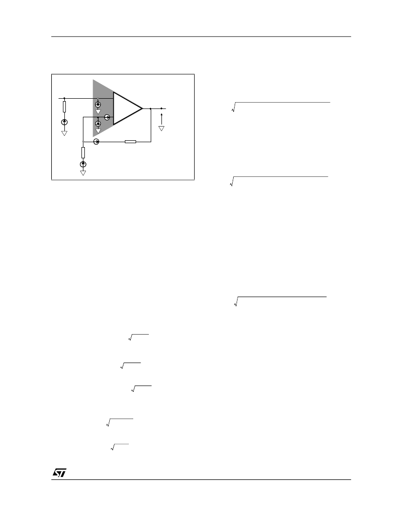
NOISE MEASUREMENT
Figure 62:
Noise Model
eN : input voltage noise of the amplifier
iNn : negative input current noise of the amplifier
iNp : positive input current noise of the amplifier
The closed loop gain is :
The six noise sources are :
We assume that the thermal noise of a resistance
R is:
4kTR
F
wher
F is the specified bandwidth.
On 1Hz bandwidth the thermal noise is reduced to
4kTR
k is the Boltzmann’s constant, equal to
1,374.10-23J/°K. T is the temperature (°K).
The output noise eNo is calculated using the Su-
perposition Theorem. However it is not the simple
sum of all noise sources. The square root of the
sum of the square of each noise source.
V12
+
+
=
eNo
2
The input noise of the instrumentation must be ex-
tracted from the measured noise value. The real
output noise value of the driver is:
The input noise is called the Equivalent Input
Noise as it is not directly measured but it is evalu-
ated from the measurement of the output divided
by the closed loop gain (eNo/g).
After simplification of the fourth and the fifth term
of (eq2) we obtain:
eNo
2
+
×
=
Measurement of eN:
We assume a short-circuit on the non-inverting in-
put (R3=0). (eq4) comes:
In order to easily extract the value of eN, the resis-
tance R2 will be chosen as low as possible. In the
other hand, the gain must be large enough.
R1=10
,
R2=910
,
R3=0, Gain=92
Equivalent Input Noise: 2.57nV/
√
Hz
Input Voltage Noise: eN=2.5nV/
√
Hz
Measurement of iNn:
R3=0 and the output noise equation is still the
(eq5). This time the gain must be decreased to de-
crease the thermal noise contribution.
R1=100
,
R2=910
,
R3=0, Gain=10.1
Equivalent Input Noise: 3.40nV/
√
Hz
Negative Input Current Noise: iNn =21pA/
√
Hz
Measurement of iNp:
To extract iNp from (eq3), a resistance R3 is con-
nected to the non-inverting input. The value of R3
must be chosen in order to keep its thermal noise
+
_
R3
R1
output
R2
iN-
iN+
8nV/
√
Hz
N1
N2
N3
TS616
eN
HP3577
Input noise:
AV
g
1
Rg
+
=
=
V
1
eN
1
2
R
1
------
+
×
=
V
2
iNn
R
2
×
=
V
3
iNp
R
3
1
2
R
1
------
+
×
×
=
V
4
2
R
1
------
4
kTR
1
×
–
=
V
5
4
kTR
2
=
V
6
1
2
R
1
------
+
4
kTR
3
=
eNo
V22
V32
V42
V52
V62
+
+
+
eq1
(
)
,
eN
2
g
2
iNn
2
R
22
iNp
2
2
+
×
+
×
R
32
×
g
2
×
=
…
2
R
1
------
2
4
kTR
1
4
kTR
2
1
2
R
1
------
+
4
kTR
3
×
+
+
×
eq
2
(
)
,
+
eNo
Measured
(
)
2
instrumentation
(
)
2
–
eq3
(
)
,
=
eN
2
g
2
iNn
2
R
22
2
iNp
2
+
×
R
32
×
g
2
×
…
g
4
kTR
2
1
2
R
1
------
+
4
kTR
3
×
+
×
eq
4
(
)
,
+
eNo
eN
2
g
2
iNn
2
R
22
g
4
kTR
2
×
+
×
+
×
eq
5
(
)
,
=
相關(guān)PDF資料 |
PDF描述 |
|---|---|
| TS61C23CXRF | Voltage Detector |
| TS61C24CXRF | Voltage Detector |
| TS61C25CXRF | Voltage Detector |
| TS61C27CXRF | Voltage Detector |
| TS61C30CXRF | Voltage Detector |
相關(guān)代理商/技術(shù)參數(shù) |
參數(shù)描述 |
|---|---|
| TS617ID | 功能描述:運(yùn)算放大器 - 運(yùn)放 DUAL WIDEBAND HIGH OUTPUT CURRENT OPAMP RoHS:否 制造商:STMicroelectronics 通道數(shù)量:4 共模抑制比(最小值):63 dB 輸入補(bǔ)償電壓:1 mV 輸入偏流(最大值):10 pA 工作電源電壓:2.7 V to 5.5 V 安裝風(fēng)格:SMD/SMT 封裝 / 箱體:QFN-16 轉(zhuǎn)換速度:0.89 V/us 關(guān)閉:No 輸出電流:55 mA 最大工作溫度:+ 125 C 封裝:Reel |
| TS617IDT | 功能描述:運(yùn)算放大器 - 運(yùn)放 Dual wideband Hi-output Amp. RoHS:否 制造商:STMicroelectronics 通道數(shù)量:4 共模抑制比(最小值):63 dB 輸入補(bǔ)償電壓:1 mV 輸入偏流(最大值):10 pA 工作電源電壓:2.7 V to 5.5 V 安裝風(fēng)格:SMD/SMT 封裝 / 箱體:QFN-16 轉(zhuǎn)換速度:0.89 V/us 關(guān)閉:No 輸出電流:55 mA 最大工作溫度:+ 125 C 封裝:Reel |
| TS61C20CXRF | 制造商:TSC 制造商全稱:Taiwan Semiconductor Company, Ltd 功能描述:Voltage Detector |
| TS61C23CXRF | 制造商:TSC 制造商全稱:Taiwan Semiconductor Company, Ltd 功能描述:Voltage Detector |
| TS61C24CXRF | 制造商:TSC 制造商全稱:Taiwan Semiconductor Company, Ltd 功能描述:Voltage Detector |
發(fā)布緊急采購(gòu),3分鐘左右您將得到回復(fù)。