- 您現(xiàn)在的位置:買賣IC網(wǎng) > PDF目錄98287 > TS8387MF 1-CH 8-BIT PROPRIETARY METHOD ADC, PARALLEL ACCESS, CQFP68 PDF資料下載
參數(shù)資料
| 型號(hào): | TS8387MF |
| 元件分類: | ADC |
| 英文描述: | 1-CH 8-BIT PROPRIETARY METHOD ADC, PARALLEL ACCESS, CQFP68 |
| 封裝: | CERAMIC, QFP-68 |
| 文件頁數(shù): | 20/38頁 |
| 文件大?。?/td> | 617K |
| 代理商: | TS8387MF |
第1頁第2頁第3頁第4頁第5頁第6頁第7頁第8頁第9頁第10頁第11頁第12頁第13頁第14頁第15頁第16頁第17頁第18頁第19頁當(dāng)前第20頁第21頁第22頁第23頁第24頁第25頁第26頁第27頁第28頁第29頁第30頁第31頁第32頁第33頁第34頁第35頁第36頁第37頁第38頁
TS8387
27/38
7.3.
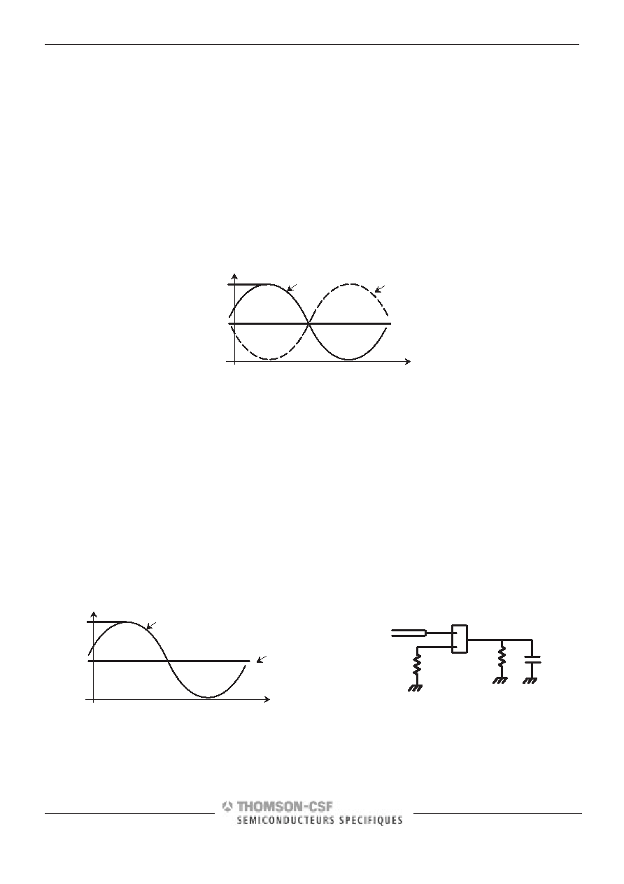
CLOCK INPUTS (CLK) (CLKB)
7.3.1.DIFFERENTIAL ECL CLOCKS INPUTS
The ADC clock input buffer is a differential preamplifier stage, which has been designed in order to be used either in
differential or single-ended mode.
The clock inputs were intended to be driven differentially with nominal –0.8V / –1.8V ECL levels.
In this mode, a low phase noise sinewave generator can be used for driving the clock inputs, followed by a power splitter
( hybrid junction ) in order to obtain 180 degrees out of phase sinewave signals. Biasing tees can be used for offseting
the common mode voltage to ECL levels.
Note : As the biasing tees propagation times are not matching, a tunable delay line is required in order to ensure the
signals to be 180 degrees out of phase.
Differential Clock inputs (ECL Levels)
–0.8V
[mV]
t
–1.8V
VCLKB
VCLK
Common mode = –1.3 V
7.3.2.SINGLE ENDED ECL CLOCK INPUT
The TS8387 can be clocked at full speed without noticeable performance degradation in either differential or single
ended configuration, using clock input ECL levels.
This is explained by the fact the ADC uses a differential preamplifier stage for the clock buffer, which has been designed
in order to be entered either in differential or single-ended mode.
This is true so long as the out of phase clock input pad is 50 ohms terminated very closely to one of the neighbouring
shield ground pad, which acts as the local Ground reference for the inphase clock input .
In single-ended configuration enter on CLK ( resp. CLKB ) pad , with the inverted phase Clock input pad CLKB (resp.
CLK) grounded.
The inphase input amplitude is 1 Volt peak to peak, centered on –1.3 Volt common mode.
The inverted phase clock input is grounded through the 50 ohms termination resistor.
Single ended Clock input (ECL):
VCLK common mode = –1.3 Volt.
VCLKB = –1.3 Volt
–0.8V
[V]
t
–1.8V
VCLK
VCLKB = –1.3 V
CLK or CLKB
CLK or CLKB double pad
50
(external)
50
reverse termination
1M
0.4 pF
相關(guān)PDF資料 |
PDF描述 |
|---|---|
| TS8387CF | 1-CH 8-BIT PROPRIETARY METHOD ADC, PARALLEL ACCESS, CQFP68 |
| TS(X)8387CF | 1-CH 8-BIT PROPRIETARY METHOD ADC, PARALLEL ACCESS, CQFP68 |
| TS8387CF_ | 1-CH 8-BIT PROPRIETARY METHOD ADC, PARALLEL ACCESS, CQFP68 |
| TS(X)8387CF_ | 1-CH 8-BIT PROPRIETARY METHOD ADC, PARALLEL ACCESS, CQFP68 |
| TS8387VF | 1-CH 8-BIT PROPRIETARY METHOD ADC, PARALLEL ACCESS, CQFP68 |
相關(guān)代理商/技術(shù)參數(shù) |
參數(shù)描述 |
|---|---|
| TS8388B | 制造商:ATMEL 制造商全稱:ATMEL Corporation 功能描述:ADC 8-bit 1 GSPS |
| TS8388BCF | 制造商:e2v technologies 功能描述:ADC 8-BIT 1 GSPS - Trays |
| TS8388BCFS | 制造商:e2v technologies 功能描述:ADC 8-BIT 1 GSPS - Trays |
| TS8388BCG | 制造商:未知廠家 制造商全稱:未知廠家 功能描述:A/D CONVERTER |
| TS8388BCGL | 制造商:e2v technologies 功能描述:ADC 8-BIT 1 GSPS - Trays |
發(fā)布緊急采購,3分鐘左右您將得到回復(fù)。