- 您現(xiàn)在的位置:買賣IC網(wǎng) > PDF目錄98302 > TSC2100IRHBG4 (TEXAS INSTRUMENTS INC) SPECIALTY CONSUMER CIRCUIT, PQCC32 PDF資料下載
參數(shù)資料
| 型號: | TSC2100IRHBG4 |
| 廠商: | TEXAS INSTRUMENTS INC |
| 元件分類: | 消費家電 |
| 英文描述: | SPECIALTY CONSUMER CIRCUIT, PQCC32 |
| 封裝: | 5 X 5 MM, GREEN, PLASTIC, QFN-32 |
| 文件頁數(shù): | 52/77頁 |
| 文件大小: | 1079K |
| 代理商: | TSC2100IRHBG4 |
第1頁第2頁第3頁第4頁第5頁第6頁第7頁第8頁第9頁第10頁第11頁第12頁第13頁第14頁第15頁第16頁第17頁第18頁第19頁第20頁第21頁第22頁第23頁第24頁第25頁第26頁第27頁第28頁第29頁第30頁第31頁第32頁第33頁第34頁第35頁第36頁第37頁第38頁第39頁第40頁第41頁第42頁第43頁第44頁第45頁第46頁第47頁第48頁第49頁第50頁第51頁當(dāng)前第52頁第53頁第54頁第55頁第56頁第57頁第58頁第59頁第60頁第61頁第62頁第63頁第64頁第65頁第66頁第67頁第68頁第69頁第70頁第71頁第72頁第73頁第74頁第75頁第76頁第77頁
TSC2100
SLAS378 NOVEMBER 2003
www.ti.com
56
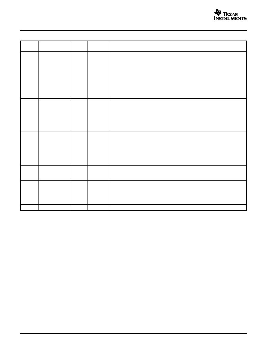
REGISTER 1EH: Audio Control 5
BIT
NAME
READ/
WRITE
RESET
VALUE
FUNCTION
D15D9
MAX_AGC_PGA
R/W
1111111
MAX ADC PGA applicable for AGC
0000000 => 0 dB
0000001 => 0.5 dB
0000010 => 1.0 dB
1110110 => 59.0 dB
1110111 => 59.5 dB
1111000 => 59.5 dB
1111111 => 59.5 dB
D8D6
AGC_NOI_DEB
R/W
000
AGC Debounce time for speech mode to silence mode transition
000 => 0 ms
001 => 0.5 ms
010 => 1.0 ms
110 => 16.0 ms
111 => 32.0 ms
D5D3
AGC_SIG_DEB
R/W
000
AGC Debounce time for silence mode to speech mode transition
000 => 0 ms
001 => 0.5 ms
010 => 1.0 ms
110 => 16.0 ms
111 => 32.0 ms
D2
DRV_POP_DIS
R/W
0
Audio Output Driver POP reduction enable
0 => Enabled
1 => Disabled
D1
DRV_POP_LEN
R/W
0
Audio Output Driver POP reduction duration
0 => Output driver ramps to final voltage in approximately 1 msec, if VGND is
powered (0.8 sec otherwise)
1 => Output driver ramps to final voltage in approximately 5 msec, if VGND is
powered (4 sec otherwise)
D0
Reserved
R
0
Reserved. Do not write 1 to this location.
LAYOUT
The following layout suggestions should provide optimum performance from the TSC2100. However, many portable
applications have conflicting requirements concerning power, cost, size, and weight. In general, most portable devices
have fairly clean power and grounds because most of the internal components are very low power. This situation means
less bypassing for the converter power and less concern regarding grounding. Still, each situation is unique and the
following suggestions should be reviewed carefully.
For optimum performance, care must be taken with the physical layout of the TSC2100 circuitry. The basic SAR architecture
is sensitive to glitches or sudden changes on the power supply, reference, ground connections, and digital inputs that occur
just prior to latching the output of the analog comparator. Therefore, during any single conversion for an n-bit SAR converter,
there are n windows in which large external transient voltages can easily affect the conversion result. Such glitches might
originate from switching power supplies, nearby digital logic, and high power devices. The degree of error in the digital
output depends on the reference voltage, layout, and the exact timing of the external event. The error can change if the
external event changes in time with respect to the timing of the critical n windows.
With this in mind, power to the TSC2100 must be clean and well bypassed. A 0.1-F ceramic bypass capacitor must be
placed as close to the device as possible. A 1-F to 10-F capacitor may also be needed if the impedance between the
TSC2100 supply pins and the system power supply is high.
A bypass capacitor on the VREF pin is generally not needed because the reference is buffered by an internal op-amp,
although it can be useful to reduce reference noise level. If an external reference voltage originates from an op-amp, make
sure that it can drive any bypass capacitor that is used without oscillation.
相關(guān)PDF資料 |
PDF描述 |
|---|---|
| TSC2100IRHBRG4 | SPECIALTY CONSUMER CIRCUIT, PQCC32 |
| TSC2101IRGZR | SPECIALTY CONSUMER CIRCUIT, PQCC48 |
| TSC2101IRGZ | SPECIALTY CONSUMER CIRCUIT, PQCC48 |
| TSC2101IRGZRG4 | SPECIALTY CONSUMER CIRCUIT, PQCC48 |
| TSC2101IRGZG4 | SPECIALTY CONSUMER CIRCUIT, PQCC48 |
相關(guān)代理商/技術(shù)參數(shù) |
參數(shù)描述 |
|---|---|
| TSC2100IRHBR | 功能描述:觸摸屏轉(zhuǎn)換器和控制器 Prog 4-Wire w/Ster Codec & Hdph/Spk Amp RoHS:否 制造商:Microchip Technology 類型:Resistive Touch Controllers 輸入類型:3 Key 數(shù)據(jù)速率:140 SPS 分辨率:10 bit 接口類型:4-Wire, 5-Wire, 8-Wire, I2C, SPI 電源電壓:2.5 V to 5.25 V 電源電流:17 mA 工作溫度:- 40 C to + 85 C 封裝 / 箱體:SSOP-20 |
| TSC2100IRHBRG4 | 功能描述:觸摸屏轉(zhuǎn)換器和控制器 Prog 4-Wire w/Ster Codec & Hdph/Spk Amp RoHS:否 制造商:Microchip Technology 類型:Resistive Touch Controllers 輸入類型:3 Key 數(shù)據(jù)速率:140 SPS 分辨率:10 bit 接口類型:4-Wire, 5-Wire, 8-Wire, I2C, SPI 電源電壓:2.5 V to 5.25 V 電源電流:17 mA 工作溫度:- 40 C to + 85 C 封裝 / 箱體:SSOP-20 |
| TSC2100IRHBRMULT1 | 制造商:Texas Instruments 功能描述: |
| TSC2101 | 制造商:TI 制造商全稱:Texas Instruments 功能描述:AUDIO CODEC WITH INTERATED HEADPHONE SPEAKER AMPLIFIER AND TOUCH SCREEN CONTROLLER |
| TSC2101_07 | 制造商:TI 制造商全稱:Texas Instruments 功能描述:AUDIO CODEC WITH INTEGRATED HEADPHONE, SPEAKER AMPLIFIER AND TOUCH SCREEN CONTROLLER |
發(fā)布緊急采購,3分鐘左右您將得到回復(fù)。