- 您現(xiàn)在的位置:買賣IC網(wǎng) > PDF目錄365968 > TSC21020F-20SA-E IC CYCLONE III FPGA 40K 324FBGA PDF資料下載
參數(shù)資料
| 型號: | TSC21020F-20SA-E |
| 英文描述: | IC CYCLONE III FPGA 40K 324FBGA |
| 中文描述: | 數(shù)字信號處理器| 32位|的CMOS | RAD數(shù)據(jù)通信硬|美巡賽| 223PIN |陶瓷 |
| 文件頁數(shù): | 7/51頁 |
| 文件大小: | 763K |
| 代理商: | TSC21020F-20SA-E |
第1頁第2頁第3頁第4頁第5頁第6頁當前第7頁第8頁第9頁第10頁第11頁第12頁第13頁第14頁第15頁第16頁第17頁第18頁第19頁第20頁第21頁第22頁第23頁第24頁第25頁第26頁第27頁第28頁第29頁第30頁第31頁第32頁第33頁第34頁第35頁第36頁第37頁第38頁第39頁第40頁第41頁第42頁第43頁第44頁第45頁第46頁第47頁第48頁第49頁第50頁第51頁
7
TSC21020F
4153F
–
AERO
–
06/03
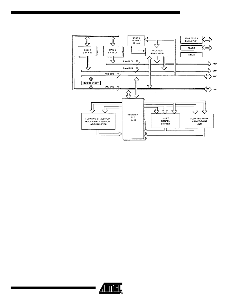
Figure 1.
TSC21020F Block Diagram
With a large number of buses connecting the registers to the computation units, data
flow between computation units and from/to off-chip memory is unconstrained and free
from bottlenecks. The 10-port register file and Harvard architecture of the TSC21020F
allow the following nine data transfers to be performed every cycle:
Off-chip read/write of two operands to or from the register file
Two operands supplied to the ALU
Two operands supplied to the multiplier
Two results received from the ALU and multiplier (three, if the ALU operation is a
combined addition/subtraction).
The processor's 48-bit orthogonal instruction word supports fully parallel data transfer
and arithmetic operations in the same instruction.
Address Generators and
Program Sequencer
Two dedicated address generators and a program sequencer supply addresses for
memory accesses. Because of this, the computation units need never be used to calcu-
late addresses. Because of its instruction cache, the TSC21020F can simultaneously
fetch an instruction and data values from both off-chip program memory and off-chip
data memory in a single cycle.
The data address generators (DAGs) provide memory addresses when external mem-
ory data is transferred over the parallel memory ports to or from internal registers. Dual
data address generators enable the processor to output two simultaneous addresses for
dual operand reads and writes. DAG 1 supplies 32-bit addresses to data memory. DAG
2 supplies 24-bit addresses to program memory for program memory data accesses.
Each DAG keeps track of up to eight address pointers, eight modifiers, eight buffer
length values and eight base values. A pointer used for indirect addressing can be mod-
ified by a value in a specified register, either before (premodify) or after (post-modify)
相關PDF資料 |
PDF描述 |
|---|---|
| TSC21020F-20SAP833 | FPGA, CYCLONE III, 40K LE, 324FBGA Programmable Logic Type:FPGA; Logic IC function:FPGA; Logic IC family:Cyclone III; Logic IC Base Number:3; I/O lines, No. of:195; |
| TSC21020F-20SASB | IC CYCLONE III FPGA 40K 324 FBGA |
| TSC21020F-20SASC | IC CYCLONE III FPGA 40K 484FBGA |
| TSC21020F-20SASL1 | IC CYCLONE III FPGA 40K 484FBGA |
| TSC21020F-20SASL2 | IC CYCLONE III FPGA 40K 484 FBGA |
相關代理商/技術參數(shù) |
參數(shù)描述 |
|---|---|
| TSC21020F-20SAP833 | 制造商:未知廠家 制造商全稱:未知廠家 功能描述:DSP|32-BIT|CMOS| RAD HARD|PGA|223PIN|CERAMIC |
| TSC21020F-20SASB | 制造商:未知廠家 制造商全稱:未知廠家 功能描述:DSP|32-BIT|CMOS| RAD HARD|PGA|223PIN|CERAMIC |
| TSC21020F-20SASC | 制造商:未知廠家 制造商全稱:未知廠家 功能描述:DSP|32-BIT|CMOS| RAD HARD|PGA|223PIN|CERAMIC |
| TSC21020F-20SASL1 | 制造商:未知廠家 制造商全稱:未知廠家 功能描述:DSP|32-BIT|CMOS| RAD HARD|PGA|223PIN|CERAMIC |
| TSC21020F-20SASL2 | 制造商:未知廠家 制造商全稱:未知廠家 功能描述:DSP|32-BIT|CMOS| RAD HARD|PGA|223PIN|CERAMIC |
發(fā)布緊急采購,3分鐘左右您將得到回復。