- 您現(xiàn)在的位置:買賣IC網 > PDF目錄225404 > UCC3580N-3 (TEXAS INSTRUMENTS INC) 1.2 A SWITCHING CONTROLLER, 430 kHz SWITCHING FREQ-MAX, PDIP16 PDF資料下載
參數資料
| 型號: | UCC3580N-3 |
| 廠商: | TEXAS INSTRUMENTS INC |
| 元件分類: | 穩(wěn)壓器 |
| 英文描述: | 1.2 A SWITCHING CONTROLLER, 430 kHz SWITCHING FREQ-MAX, PDIP16 |
| 封裝: | GREEN, PLASTIC, DIP-16 |
| 文件頁數: | 12/19頁 |
| 文件大小: | 761K |
| 代理商: | UCC3580N-3 |
2
UCC1580-1,-2,-3,-4
UCC2580-1,-2,-3,-4
UCC3580-1,-2,-3,-4
VDD ...........................................16V
IVDD.......................................... 25mA
LINE, RAMP ........................ 0.3V to VDD + 1V
ILINE,IRAMP .....................................5mA
DELAY ........................................ 5.3V
IDELAY ........................................ 5mA
IOUT1 (tpw < 1 s and Duty Cycle < 10%) ....... 0.6A to 1.2A
IOUT2 (tpw < 1 s and Duty Cycle < 10%) ....... 0.4A to 0.4A
ICLK................................ 100mA to 100mA
OSC1, OSC2, SS, SHTDWN, EAIN ..... 0.3V to REF + 0.3V
IEAOUT.................................. 5mAto5mA
IREF ......................................... 30mA
PGND .................................. 0.2V to 0.2V
Storage Temperature .................. -65°C to +150°C
Junction Temperature .................. -55°C to +150°C
Lead Temperature (Soldering, 10 sec.) ............. +300°C
All voltages are with respect to ground unless otherwise stated.
Currents are positive into, negative out of the specified termi-
nal. Consult Packaging Section of Databook for thermal limita-
tions and considerations of packages.
ABSOLUTE MAXIMUM RATINGS
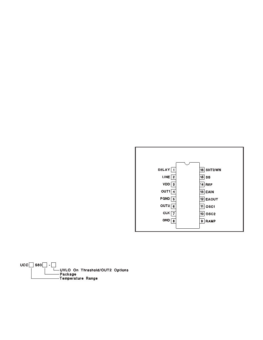
CONNECTION DIAGRAMS
DIL-16, SOIC-16 (Top View)
J, N, or D Packages
ORDER INFORMATION
The main gate drive output (OUT1) is controlled by the
pulse width modulator. The second output (OUT2) is in-
tended to activate an auxiliary switch during the off time
of the main switch, except that between each transition
there is deadtime where both switches are off, pro-
grammed by a single external resistor. This design offers
two options for OUT2, normal and inverted. In the -1 and
-2 versions, OUT2 is normal and can be used to drive
PMOS FETs. In the -3 and -4 versions, OUT2 is inverted
and can be used to drive NMOS FETs. In all versions,
both the main and auxiliary switches are held off prior to
startup and when the PWM command goes to zero duty
cycle. During fault conditions, OUT1 is held off while
OUT2 operates at maximum duty cycle with a guaran-
teed off time equal to the sum of the two deadtimes.
Undervoltage lockout monitors supply voltage (VDD), the
precision reference (REF), input line voltage (LINE), and
the shutdown comparator (SHTDWN).
If after any of
these four have sensed a fault condition, recovery to full
operation is initiated with a soft start. VDD thresholds, on
and off, are 15V and 8.5V for the -2 and -4 versions, 9V
and 8.5V for the -1 and -3 versions.
The UCC1580-x is specified for operation over the mili-
tary
temperature
range
of -55°C to 125°C. The
UCC2580-x is specified from -40°C to 85°C. The
UCC3580-x is specified from 0°C to 70°C. Package op-
tions include 16-pin surface mount and dual in-line.
DESCRIPTION (cont.)
相關PDF資料 |
PDF描述 |
|---|---|
| UCC3813PW-2 | 1 A SWITCHING CONTROLLER, 52 kHz SWITCHING FREQ-MAX, PDSO8 |
| UCC3813PW-4G4 | 1 A SWITCHING CONTROLLER, 52 kHz SWITCHING FREQ-MAX, PDSO8 |
| UCC3813D-0G4 | 1 A SWITCHING CONTROLLER, 52 kHz SWITCHING FREQ-MAX, PDSO8 |
| UCC3941-5D | SWITCHING REGULATOR, PDSO8 |
| UCC3941-ADJJ | SWITCHING REGULATOR, CDIP8 |
相關代理商/技術參數 |
參數描述 |
|---|---|
| UCC3580N-3G4 | 功能描述:電壓模式 PWM 控制器 Single Ended Active Clamp/Reset PWM RoHS:否 制造商:Texas Instruments 輸出端數量:1 拓撲結構:Buck 輸出電壓:34 V 輸出電流: 開關頻率: 工作電源電壓:4.5 V to 5.5 V 電源電流:600 uA 最大工作溫度:+ 125 C 最小工作溫度:- 40 C 封裝 / 箱體:WSON-8 封裝:Reel |
| UCC3580N-4 | 功能描述:電壓模式 PWM 控制器 Single Ended Active Clamp/Reset PWM RoHS:否 制造商:Texas Instruments 輸出端數量:1 拓撲結構:Buck 輸出電壓:34 V 輸出電流: 開關頻率: 工作電源電壓:4.5 V to 5.5 V 電源電流:600 uA 最大工作溫度:+ 125 C 最小工作溫度:- 40 C 封裝 / 箱體:WSON-8 封裝:Reel |
| UCC3580N-4G4 | 功能描述:電壓模式 PWM 控制器 Single Ended Active Clamp/Reset PWM RoHS:否 制造商:Texas Instruments 輸出端數量:1 拓撲結構:Buck 輸出電壓:34 V 輸出電流: 開關頻率: 工作電源電壓:4.5 V to 5.5 V 電源電流:600 uA 最大工作溫度:+ 125 C 最小工作溫度:- 40 C 封裝 / 箱體:WSON-8 封裝:Reel |
| UCC3580Q-1 | 制造商:未知廠家 制造商全稱:未知廠家 功能描述: |
| UCC3580Q-2 | 制造商:未知廠家 制造商全稱:未知廠家 功能描述:Voltage-Mode SMPS Controller |
發(fā)布緊急采購,3分鐘左右您將得到回復。