- 您現(xiàn)在的位置:買賣IC網(wǎng) > PDF目錄379492 > UPC3025HB (NEC Corp.) LOW-SATURATION STABILIZED POWER SUPPLY WITH ON/OFF FUNCTION (1 A OUTPUT) PDF資料下載
參數(shù)資料
| 型號(hào): | UPC3025HB |
| 廠商: | NEC Corp. |
| 英文描述: | LOW-SATURATION STABILIZED POWER SUPPLY WITH ON/OFF FUNCTION (1 A OUTPUT) |
| 中文描述: | 低飽和度對(duì)穩(wěn)壓電源開/關(guān)功能(1 A輸出) |
| 文件頁(yè)數(shù): | 3/12頁(yè) |
| 文件大?。?/td> | 76K |
| 代理商: | UPC3025HB |
Data Sheet G15506EJ2V0DS
3
μ
PC3018, 3025
ABSOLUTE MAXIMUM RATINGS
(T
A
= 25°C unless otherwise specified)
Parameter
Symbol
Rating
Unit
Input Voltage
V
IN
–0.3 to +20
V
ON/OFF pin voltage
V
ON/OFF
–0.3 to V
IN
+0.3 V (however, V
ON/OFF
≤
20)
Internal Power Dissipation (T
C
= 25
°
C)
P
T
10
Note
W
Operating Ambient Temperature
T
A
–30 to +85
°C
Operating Junction Temperature
T
J
–30 to +150
°C
Storage Temperature
T
stg
–55 to +150
°C
Thermal Resistance (junction to case)
R
th(J-C)
12.5
°C/W
Thermal Resistance (junction to ambient)
R
th(J-A)
125
°C/W
Note
The total dissipation is limited by an internal circuit. Where T
J
> 150°C, an internal protection circuit cuts off the
output.
Caution Product quality may suffer if the absolute maximum rating is exceeded even momentarily for any
parameter. That is, the absolute maximum ratings are rated values at which the product is on the verge
of suffering physical damage, and therefore the product must be used under conditions that ensure that
the absolute maximum ratings are not exceeded.
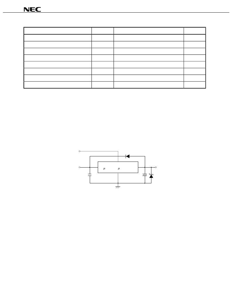
TYPICAL CONNECTION
INPUT
C
IN
PC3018, PC3025
OUTPUT
C
OUT
D
1
D
2
+
ON/OFF
C
IN
:
Must be 0.1
μ
F or more. Determine the capacitance in accordance with the line between the power supply
smoothing circuit and input pin. Be sure to connect this capacitor to prevent abnormal oscillation. Use of a
capacitor with excellent voltage and temperature characteristics, such as a film capacitor, is recommended. Note
that some laminated ceramic capacitors have poor temperature and voltage characteristics. When using a
laminated ceramic capacitor, the capacitance of 0.1
μ
F or more must be reserved in the voltage and temperature
ranges used.
C
OUT
: Must be 10
μ
F or more. Be sure to connect this capacitor to prevent oscillation and to improve transient load
stability.
Connect C
IN
and C
OUT
as close to the IC pins as possible (within 1 to 2 cm). Also, when using the device at 0
°
C or
less, use an electrolytic capacitor with low impedance characteristics.
D
1
:
Connect a diode if the voltage on the OUTPUT pin is higher than that on the INPUT pin.
D
2
:
Connect a Schottky barrier diode if the voltage on the OUTPUT pin is lower than that on the GND pin.
Caution
Ensure that voltage is not applied to the OUTPUT pin externally.
Supply V
IN
and V
ON/OFF
from different power supplies.
Design so that V
IN
and V
ON/OFF
either rise at the same time or V
ON/OFF
rises after V
IN
.
相關(guān)PDF資料 |
PDF描述 |
|---|---|
| UPC3025TJ | LOW-SATURATION STABILIZED POWER SUPPLY WITH ON/OFF FUNCTION (1 A OUTPUT) |
| UPC3018TJ-E2 | LOW-SATURATION STABILIZED POWER SUPPLY WITH ON/OFF FUNCTION (1 A OUTPUT) |
| UPC337HF | TRANSISTOR DUAL NPN/PNP SOT-563 |
| UPC337 | 3-TERMINAL NEGATIVE ADJUSTABLE REGULATOR |
| UPC339G2 | LOW POWER QUAD COMPARATOR |
相關(guān)代理商/技術(shù)參數(shù) |
參數(shù)描述 |
|---|---|
| UPC3025TJ | 制造商:NEC 制造商全稱:NEC 功能描述:LOW-SATURATION STABILIZED POWER SUPPLY WITH ON/OFF FUNCTION (1 A OUTPUT) |
| UPC3025TJ(AZ) | 制造商:Renesas Electronics Corporation 功能描述: |
| UPC3025TJ-E1 | 制造商:NEC 制造商全稱:NEC 功能描述:LOW-SATURATION STABILIZED POWER SUPPLY WITH ON/OFF FUNCTION (1 A OUTPUT) |
| UPC3025TJ-E2 | 制造商:NEC 制造商全稱:NEC 功能描述:LOW-SATURATION STABILIZED POWER SUPPLY WITH ON/OFF FUNCTION (1 A OUTPUT) |
| UPC3033H(AZ) | 制造商:Renesas Electronics Corporation 功能描述: |
發(fā)布緊急采購(gòu),3分鐘左右您將得到回復(fù)。