- 您現(xiàn)在的位置:買(mǎi)賣(mài)IC網(wǎng) > PDF目錄245264 > UPD121A10T1F-E2-AT 1 V FIXED POSITIVE REGULATOR, PSSO4 PDF資料下載
參數(shù)資料
| 型號(hào): | UPD121A10T1F-E2-AT |
| 元件分類(lèi): | 固定正電壓?jiǎn)温份敵鰳?biāo)準(zhǔn)穩(wěn)壓器 |
| 英文描述: | 1 V FIXED POSITIVE REGULATOR, PSSO4 |
| 封裝: | LEAD FREE, TO-252, MP-3ZK, 6 PIN |
| 文件頁(yè)數(shù): | 4/10頁(yè) |
| 文件大小: | 208K |
| 代理商: | UPD121A10T1F-E2-AT |
Data Sheet G18843EJ1V0DS
3
μ PD121A10
CIN
: 0.1
μ F or higher. Be sure to connect CIN to prevent parasitic oscillation. Set this value according to the length
of the line between the regulator and the INPUT pin. Use of a film capacitor or other capacitor with first-rate
voltage and temperature characteristics is recommended. If using a laminated ceramic capacitor, it is
necessary to ensure that CIN is 0.1
μ F or higher for the voltage and temperature range to be used.
COUT : 10
μ F or higher. Be sure to connect COUT to prevent oscillation and improve excessive load regulation. Place
CIN and COUT as close as possible to the IC pins (within 1 to 2 cm). Use the capacitor whose capacitance value
is 10
μ F or more under use conditions.
D1
: If the OUTPUT pin has a higher voltage than the INPUT pin, connect a diode.
D2
: If the OUTPUT pin has a lower voltage than the GND pin, connect a Schottky barrier diode.
R1, R2: The total amount of R1 and R2 is sure to below 200 k
Ω (100 kΩ TYP.).
VOUT = (1
+ R1/R2) VREF
Note
Note When VOUT = 1 V: R1 = 40 k
Ω, R2 = 60 kΩ
Caution1. Make sure that no external voltage is applied to the OUTPUT pin.
2. VDD pins (Bias voltage) must be supplied in a separate power supply from that of INPUT pins (Input
voltage).
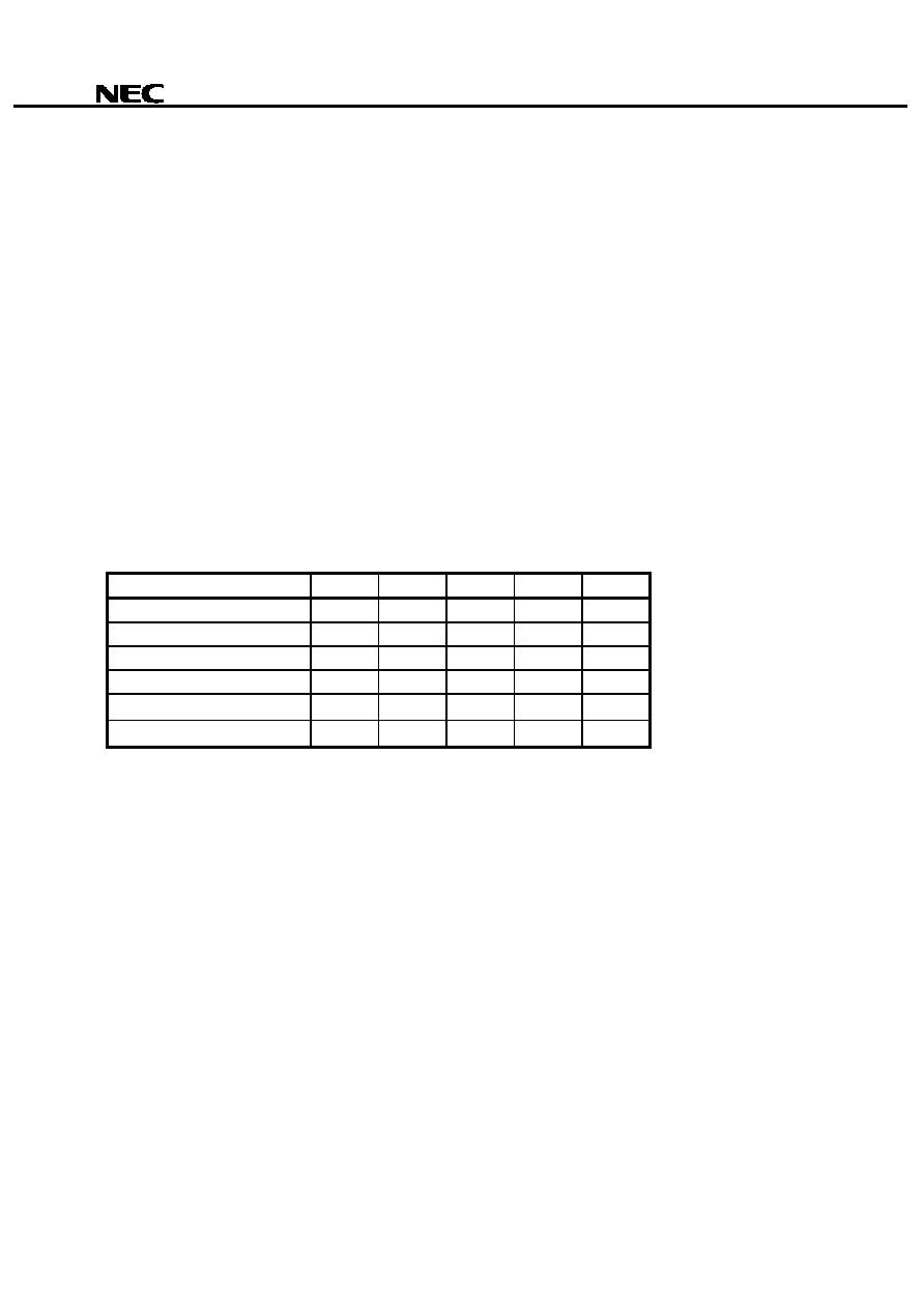
RECOMMENDED OPERATING CONDITIONS
Parameter
Symbol
MIN.
TYP.
MAX.
Unit
Input Voltage (VO = 1.0 V)
VIN
1.62
Note
2.0
2.65
V
Output Voltage
VO
0.95
1.0
1.15
V
Bias Voltage
VDD
4.0
5.0
5.5
V
Output Current
IO
0
2.0
A
Operating Ambient Temperature
TA
20
+ 85
°C
Operating Junction Temperature
TJ
20
+ 125
°C
Note It needs 1.7 V
≤ VIN ≤ 2.65 V to output IO = 2.0 A.
Caution1. Power on VIN first, and then VDD on start-up. When the power is turned off, turn off VDD first. Note
that the voltage of VDD must not be kept 3.0 V or less.
2. If absolute maximum rating is not exceeded, you can used this product above the recommended
operating range. However, since a margin with absolute maximum rating decreases, please use
this product after sufficient evaluation.
相關(guān)PDF資料 |
PDF描述 |
|---|---|
| UPD121A10T1F | 1 V FIXED POSITIVE REGULATOR, PSSO4 |
| UPC317HF | 1.3 V-30 V ADJUSTABLE POSITIVE REGULATOR, PSFM3 |
| UPC78L15T-AZ | 15 V FIXED POSITIVE REGULATOR, PSSO3 |
| UPC78N05H-AZ | 5 V FIXED POSITIVE REGULATOR, PSIP3 |
| UPC24A12HF | 12 V FIXED POSITIVE LDO REGULATOR, 1 V DROPOUT, PSFM3 |
相關(guān)代理商/技術(shù)參數(shù) |
參數(shù)描述 |
|---|---|
| UPD121W00AT1F | 制造商:NEC 制造商全稱(chēng):NEC 功能描述:MOS INTEGRATED CIRCUIT |
| UPD121W00AT1F-E1-AT | 制造商:NEC 制造商全稱(chēng):NEC 功能描述:MOS INTEGRATED CIRCUIT |
| UPD121W00AT1F-E2-AT | 制造商:NEC 制造商全稱(chēng):NEC 功能描述:MOS INTEGRATED CIRCUIT |
| UPD121W18AT1F | 制造商:NEC 制造商全稱(chēng):NEC 功能描述:MOS INTEGRATED CIRCUIT |
| UPD121W18AT1F-E1-AT | 制造商:NEC 制造商全稱(chēng):NEC 功能描述:MOS INTEGRATED CIRCUIT |
發(fā)布緊急采購(gòu),3分鐘左右您將得到回復(fù)。