- 您現(xiàn)在的位置:買賣IC網(wǎng) > PDF目錄378734 > UPD16732B (NEC Corp.) 384-OUTPUT TFT-LCD SOURCE DRIVER COMPATIBLE WITH 64-GRAY SCALES PDF資料下載
參數(shù)資料
| 型號: | UPD16732B |
| 廠商: | NEC Corp. |
| 英文描述: | 384-OUTPUT TFT-LCD SOURCE DRIVER COMPATIBLE WITH 64-GRAY SCALES |
| 中文描述: | 384輸出的TFT - LCD源驅(qū)動程序完全兼容64灰度 |
| 文件頁數(shù): | 4/24頁 |
| 文件大小: | 186K |
| 代理商: | UPD16732B |
Data Sheet S13972EJ3V0DS00
4
μ
PD16732A, 16732B
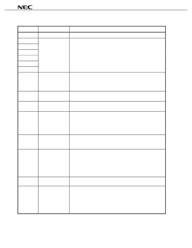
4. PIN FUNCTIONS
(1/2)
Pin Symbol
Pin Name
Description
S
1
to S
384
Driver output
The D/A converted 64-gray-scale analog voltage is output.
D
00
to D
05
D
10
to D
15
D
20
to D
25
D
30
to D
35
D
40
to D
45
D
50
to D
55
Display data input
The display data is input with a width of 36 bits, viz., the gray scale data (6 bits)
by 6 dots (2 pixels).
D
X0
: LSB, D
X5
: MSB
R,/L
Shift direction control
input
These refer to the start pulse input/output pins when driver ICs are connected in
cascade. The shift directions of the shift registers are as follows.
R,/L = H : STHR input, S
1
→
S
384
, STHL output
R,/L = L : STHL input, S
384
→
S
1
, STHR output
STHR
Right shift start pulse
input/output
R,/L = H : Becomes the start pulse input pin.
R,/L = L : Becomes the start pulse output pin.
STHL
Left shift start pulse
input/output
R,/L = H : Becomes the start pulse output pin.
R,/L = L : Becomes the start pulse input pin.
CLK
Shift clock input
Refers to the shift register’s shift clock input. The display data is incorporated into
the data register at the rising edge.
At the rising edge of the 64th clock after the start pulse input, the start pulse
output reaches the high level, thus becoming the start pulse of the next-level
driver.
STB
Latch input
The contents of the data register are transferred to the latch circuit at the rising
edge. And, at the falling edge, the gray scale voltage is supplied to the driver. It
is necessary to ensure input of one pulse per horizontal period.
POL
Polarity input
POL = L : The S
2n–1
output uses V
0
to V
4
as the reference supply. The S
2n
output
uses V
5
to V
9
as the reference supply.
POL = H: The S
2n–1
output uses V
5
to V
9
as the reference supply. The S
2n
output
uses V
0
to V
4
as the reference supply.
S
2n-1
indicates the odd output: and S
2n
indicates the even output. Input of the POL
signal is allowed the setup time (t
POL
-
STB
) with respect to STB’s rising edge.
POL2
Data inversion
POL2 = H : Display data is inverted.
POL2 = L : Display data is not inverted
LPC
Low power control input
The current consumption is lowered by controlling the constant current source of
the output amplifier. In low power mode (LPC = “L”), the V
DD2
of static current
consumption can be reduced to two thirds of the normal current consumption. This
pin is pulled up to the V
DD1
power supply inside the IC.
LPC = H or Open : Normal power mode
LPC = L : Low power mode
相關(guān)PDF資料 |
PDF描述 |
|---|---|
| UPD16732BN | 384-OUTPUT TFT-LCD SOURCE DRIVER COMPATIBLE WITH 64-GRAY SCALES |
| UPD16732BN-XXX | LCD Display Driver |
| UPD16750N-XXX | LCD Display Driver |
| UPD16750 | 384-OUTPUT TFT-LCD SOURCE DRIVER COMPATIBLE WITH 256-GRAY SCALES |
| UPD16750N | 384-OUTPUT TFT-LCD SOURCE DRIVER COMPATIBLE WITH 256-GRAY SCALES |
相關(guān)代理商/技術(shù)參數(shù) |
參數(shù)描述 |
|---|---|
| UPD16732BN | 制造商:NEC 制造商全稱:NEC 功能描述:384-OUTPUT TFT-LCD SOURCE DRIVER COMPATIBLE WITH 64-GRAY SCALES |
| UPD16732BN-XXX | 制造商:NEC 制造商全稱:NEC 功能描述:LCD Display Driver |
| UPD16732D | 制造商:未知廠家 制造商全稱:未知廠家 功能描述:UPD16732D Data Sheet | Data Sheet[06/2002] |
| UPD16732E | 制造商:未知廠家 制造商全稱:未知廠家 功能描述:UPD16732E Data Sheet | Data Sheet[06/2002] |
| UPD16732N-XXX | 制造商:未知廠家 制造商全稱:未知廠家 功能描述:LCD Display Driver |
發(fā)布緊急采購,3分鐘左右您將得到回復(fù)。