- 您現(xiàn)在的位置:買賣IC網(wǎng) > PDF目錄379496 > UPD44164364F5-E50-EQ1 (NEC Corp.) 18M-BIT DDRII SRAM 4-WORD BURST OPERATION PDF資料下載
參數(shù)資料
| 型號: | UPD44164364F5-E50-EQ1 |
| 廠商: | NEC Corp. |
| 英文描述: | 18M-BIT DDRII SRAM 4-WORD BURST OPERATION |
| 中文描述: | 1800萬位的SRAM 4條DDRII字爆發(fā)運(yùn)作 |
| 文件頁數(shù): | 8/32頁 |
| 文件大?。?/td> | 394K |
| 代理商: | UPD44164364F5-E50-EQ1 |
第1頁第2頁第3頁第4頁第5頁第6頁第7頁當(dāng)前第8頁第9頁第10頁第11頁第12頁第13頁第14頁第15頁第16頁第17頁第18頁第19頁第20頁第21頁第22頁第23頁第24頁第25頁第26頁第27頁第28頁第29頁第30頁第31頁第32頁
8
Data Sheet M15822EJ7V
1
DS
μ
PD44164084, 44164184, 44164364
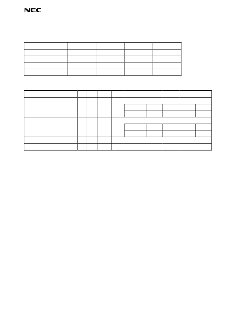
Burst Sequence
Linear Burst Sequence Table
[
μ
PD44164184,
μ
PD44164364]
A1, A0
A1, A0
A1, A0
A1, A0
External Address
0, 0
0, 1
1, 0
1, 1
1st Internal Burst Address
0, 1
1, 0
1, 1
0, 0
2nd Internal Burst Address
1, 0
1, 1
0, 0
0, 1
3rd Internal Burst Address
1, 1
0, 0
0, 1
1, 0
Truth Table
Operation
/LD
R, /W
CLK
DQ
WRITE cycle
L
L
L
→
H
Data in
Load address, input write data on two
Input data
D(A1)
D(A2)
D(A3)
D(A4)
consecutive K and /K rising edge
Input clock
K(t+1)
↑
/K(t+1)
↑
K(t+2)
↑
/K(t+2)
↑
READ cycle
L
H
L
→
H
Data out
Load address, read data on two
Output data
Q(A1)
Q(A2)
Q(A3)
Q(A4)
consecutive C and /C rising edge
Output clock
/C(t+1)
↑
C(t+2)
↑
/C(t+2)
↑
C(t+3)
↑
NOP (No operation)
H
X
L
→
H
High-Z
STANDBY(Clock stopped)
X
X
Stopped
Previous state
Remarks 1.
H : High level, L : Low level,
×
: don’t care,
↑
: rising edge.
2.
Data inputs are registered at K and /K rising edges. Data outputs are delivered at C and /C rising edges
except if C and /C are HIGH then Data outputs are delivered at K and /K rising edges.
3.
All control inputs in the truth table must meet setup/hold times around the rising edge (LOW to HIGH) of
K. All control inputs are registered during the rising edge of K.
4.
This device contains circuitry that will ensure the outputs will be in high impedance during power-up.
5.
Refer to state diagram and timing diagrams for clarification.
6.
A1 refers to the address input during a WRITE or READ cycle. A2, A3 and A4 refer to the next internal
burst address in accordance with the linear burst sequence.
7.
It is recommended that K = /K = C = /C when clock is stopped. This is not essential but permits most
rapid restart by overcoming transmission line charging symmetrically.
相關(guān)PDF資料 |
PDF描述 |
|---|---|
| UPD44164184F5-E40-EQ1 | 18M-BIT DDRII SRAM 4-WORD BURST OPERATION |
| UPD44164185F5-E50-EQ1 | 18M-BIT DDRII SRAM SEPARATE I/O 2-WORD BURST OPERATION |
| UPD44164185F5-E40-EQ1 | 18M-BIT DDRII SRAM SEPARATE I/O 2-WORD BURST OPERATION |
| UPD44164365F5-E50-EQ1 | 18M-BIT DDRII SRAM SEPARATE I/O 2-WORD BURST OPERATION |
| UPD44165082F5-E60-EQ1 | 18M-BIT QDRII SRAM 2-WORD BURST OPERATION |
相關(guān)代理商/技術(shù)參數(shù) |
參數(shù)描述 |
|---|---|
| UPD44165092BF5-E40-EQ3-A | 制造商:Renesas Electronics Corporation 功能描述:2MX9, 2BURST, 250 MHZ QDRII SRAM - Trays |
| UPD44165094BF5-E40-EQ3-A | 制造商:Renesas Electronics Corporation 功能描述:SRAM Chip Sync Dual 1.8V 18M-Bit 2M x 9-Bit 0.45ns 165-Pin BGA |
| UPD44165362BF5-E40-EQ3 | 制造商:Renesas Electronics Corporation 功能描述:UPD44165362BF5-E40-EQ3 - Trays |
| UPD44165362BF5-E40-EQ3-A | 制造商:Renesas Electronics Corporation 功能描述:SRAM Chip Sync Dual 1.8V 18M-Bit 512K x 36 0.45ns 165-Pin BGA |
| UPD44321182GF-A50(A) | 制造商:Renesas Electronics Corporation 功能描述: |
發(fā)布緊急采購,3分鐘左右您將得到回復(fù)。