- 您現(xiàn)在的位置:買賣IC網(wǎng) > PDF目錄384043 > UPD485505 (NEC Corp.) LINE BUFFER 5K-WORD BY 8-BIT PDF資料下載
參數(shù)資料
| 型號(hào): | UPD485505 |
| 廠商: | NEC Corp. |
| 英文描述: | LINE BUFFER 5K-WORD BY 8-BIT |
| 中文描述: | 行緩沖區(qū)5K - Word的8位 |
| 文件頁數(shù): | 4/20頁 |
| 文件大小: | 174K |
| 代理商: | UPD485505 |
μ
PD485505
4
Data Sheet M10059EJ7V0DS00
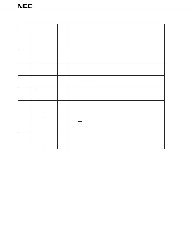
1. Input/Output Pin Function
Pin
Pin
Number
Symbol
Pin
Name
24 - 21
D
IN0
|
D
IN7
Data
Input
16 - 13
1 - 4
D
OUT0
|
D
OUT7
Data
Output
9 - 12
19
RSTW
Reset
Write
Input
6
RSTR
Reset
Read
Input
20
WE
Write
Enable
Input
5
RE
Read
Enable
Input
17
WCK
Write
Clock
Input
8
RCK
Read
Clock
Input
I/O
Function
In
Write data input pins.
The data inputs are strobed by the rising edge of WCK at the end of a cycle
and the setup and hold times (t
DS
, t
DH
) are defined at this point.
Out
Read data output pins.
The access time is regulated from the rising edge of RCK at the beginning of a
cycle and defined by t
AC
.
In
Reset input pin for the initialization of the write address pointer.
The state of RSTW is strobed by the rising edge of WCK at the beginning of a
cycle and the setup and hold times (t
RS
, t
RH
) are defined.
In
Reset input pin for the initialization of the read address pointer.
The state of RSTR is strobed by the rising edge of RCK at the beginning of a
cycle and the setup and hold times (t
RS
, t
RH
) are defined.
In
Write operation control signal input pin.
When WE is in the disable mode (“H” level), the internal write operation is
inhibited and the write address pointer stops at the current position.
In
Read operation control signal input pin.
When RE is in the disable mode (“H” level), the internal read operation is
inhibited and the read address pointer stops at the current position. The output
changes to high impedance.
In
Write clock input pin.
When WE is enabled (“L” level), the write operation is executed in
synchronization with the write clock. The write address pointer is incremented
simultaneously.
In
Read clock input pin.
When RE is enabled (“L” level), the read operation is executed in synchroniza-
tion with the read clock. The read address pointer is incremented
simultaneously.
相關(guān)PDF資料 |
PDF描述 |
|---|---|
| UPD485505G-25 | LINE BUFFER 5K-WORD BY 8-BIT |
| UPD485505G-35 | LINE BUFFER 5K-WORD BY 8-BIT |
| UPD4990A | SERIAL I/O CALENDAR & CLOCK CMOS LSI |
| UPD4990AC | SERIAL I/O CALENDAR & CLOCK CMOS LSI |
| UPD4990AG | SERIAL I/O CALENDAR & CLOCK CMOS LSI |
相關(guān)代理商/技術(shù)參數(shù) |
參數(shù)描述 |
|---|---|
| UPD485505-2G | 制造商:NEC Electronics Corporation 功能描述: |
| UPD485505G-25 | 制造商:NEC Electronics Corporation 功能描述: |
| uPD485505G-25-A | 制造商:Renesas Electronics 功能描述:18ns 5V Cut Tape |
| UPD485505G-35-A | 制造商:Renesas Electronics 功能描述:25ns 5V Cut Tape |
| UPD485506G5-25-7JF | 制造商:NEC Electronics Corporation 功能描述: 制造商:NEC Electronics Corporation 功能描述:FIELD/FRAME/LINE MEMORY, 44 Pin, Plastic, TSOP |
發(fā)布緊急采購,3分鐘左右您將得到回復(fù)。