- 您現(xiàn)在的位置:買(mǎi)賣(mài)IC網(wǎng) > PDF目錄384045 > UPD7228 (NEC Corp.) 1/8, 1/16 DUTY LCD CONTROLLER/DRIVER PDF資料下載
參數(shù)資料
| 型號(hào): | UPD7228 |
| 廠商: | NEC Corp. |
| 英文描述: | 1/8, 1/16 DUTY LCD CONTROLLER/DRIVER |
| 中文描述: | 1 / 8,1 / 16稅LCD控制器/驅(qū)動(dòng) |
| 文件頁(yè)數(shù): | 15/64頁(yè) |
| 文件大?。?/td> | 314K |
| 代理商: | UPD7228 |
第1頁(yè)第2頁(yè)第3頁(yè)第4頁(yè)第5頁(yè)第6頁(yè)第7頁(yè)第8頁(yè)第9頁(yè)第10頁(yè)第11頁(yè)第12頁(yè)第13頁(yè)第14頁(yè)當(dāng)前第15頁(yè)第16頁(yè)第17頁(yè)第18頁(yè)第19頁(yè)第20頁(yè)第21頁(yè)第22頁(yè)第23頁(yè)第24頁(yè)第25頁(yè)第26頁(yè)第27頁(yè)第28頁(yè)第29頁(yè)第30頁(yè)第31頁(yè)第32頁(yè)第33頁(yè)第34頁(yè)第35頁(yè)第36頁(yè)第37頁(yè)第38頁(yè)第39頁(yè)第40頁(yè)第41頁(yè)第42頁(yè)第43頁(yè)第44頁(yè)第45頁(yè)第46頁(yè)第47頁(yè)第48頁(yè)第49頁(yè)第50頁(yè)第51頁(yè)第52頁(yè)第53頁(yè)第54頁(yè)第55頁(yè)第56頁(yè)第57頁(yè)第58頁(yè)第59頁(yè)第60頁(yè)第61頁(yè)第62頁(yè)第63頁(yè)第64頁(yè)
Data Sheet S10299EJ4V0DS00
15
μ
PD16434
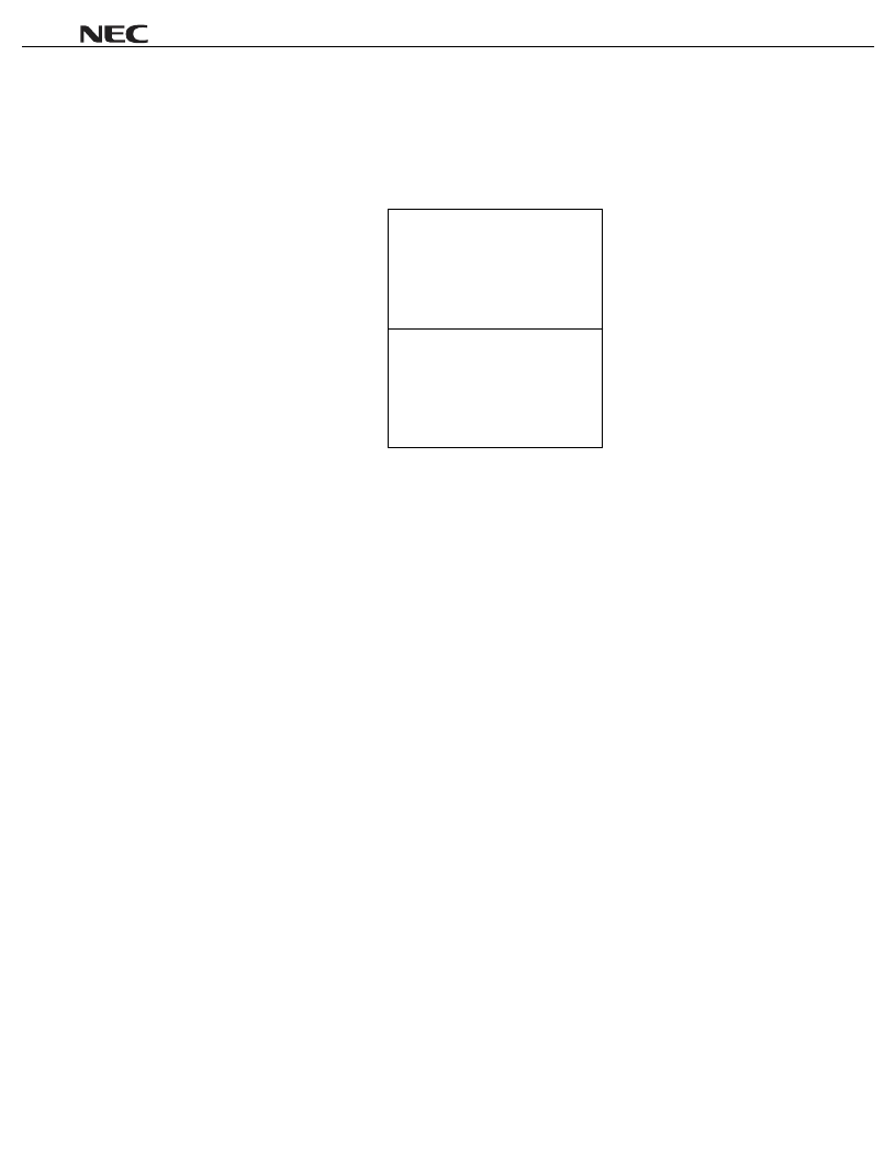
2.5 Data Memory
The data memory is a static RAM configured by two 50-word
×
8-bit banks. It is used for storing display data.
Figure 2–5. Data Memory Configuration
Bank 0
(50 x 8)
Bank 1
(50 x 8)
00H
31H
00H
31H
The data memory bank is specified by the bank flag in the data pointer, and the address in the bank is specified
by the 6-bit binary counter in the data pointer.
The 8-bit data, written to the serial/parallel interface by the CPU, is used for operation or decoded according to
the specified data processing mode, and is written into the data memory.
The data memory contents can be directly manipulated by a bit manipulation instruction.
When the
μ
PD16434 is set in the read mode, the data memory contents are output to the CPU through the
serial/parallel interface.
The data memory contents are read out in bit units in synchronization with the row drive signal and are sent to the
column driver for driving the LCD. This operation is performed independently from command/data write/read operation
with the CPU, which is performed through the serial/parallel interface. Display data read out operation differs,
depending on the number of time-divisions.
(1) 8-time-division (single/multi-chip configuration)
The contents of the display data in bank 0 or bank 1, whichever is specified by the SMM command, are read
out to the column driver.
Figure 2–6 shows bits correspondence for the row driver and column driver for the data memory. If the data
located at the Rn and Cm intersection is 1, the corresponding LCD dot is ON. If the data is 0, the dot is OFF.
相關(guān)PDF資料 |
PDF描述 |
|---|---|
| UPD7228A | 1/8, 1/16 DUTY LCD CONTROLLER/DRIVER |
| UPD7229 | 1/8, 1/16 DUTY LCD CONTROLLER/DRIVER |
| UPD7229A | 1/8, 1/16 DUTY LCD CONTROLLER/DRIVER |
| UPD16434G-001-12 | 1/8, 1/16 DUTY LCD CONTROLLER/DRIVER |
| UPD16434GF-001-3B9 | 1/8, 1/16 DUTY LCD CONTROLLER/DRIVER |
相關(guān)代理商/技術(shù)參數(shù) |
參數(shù)描述 |
|---|---|
| UPD74HC04C | 制造商:Panasonic Industrial Company 功能描述:IC |
| UPD750068GT-396 | 制造商:Renesas Electronics Corporation 功能描述: |
| UPD7507C189 | 制造商:Panasonic Industrial Company 功能描述:IC |
| UPD7508CU265 | 制造商:Panasonic Industrial Company 功能描述:IC |
| UPD75208 | 制造商:Panasonic Industrial Company 功能描述:IC |
發(fā)布緊急采購(gòu),3分鐘左右您將得到回復(fù)。