- 您現(xiàn)在的位置:買賣IC網(wǎng) > PDF目錄379503 > UPD75306BGK (NEC Corp.) 4-BIT SINGLE-CHIP MICROCOMPUTER PDF資料下載
參數(shù)資料
| 型號(hào): | UPD75306BGK |
| 廠商: | NEC Corp. |
| 英文描述: | 4-BIT SINGLE-CHIP MICROCOMPUTER |
| 中文描述: | 4位單片機(jī) |
| 文件頁數(shù): | 11/76頁 |
| 文件大小: | 572K |
| 代理商: | UPD75306BGK |
第1頁第2頁第3頁第4頁第5頁第6頁第7頁第8頁第9頁第10頁當(dāng)前第11頁第12頁第13頁第14頁第15頁第16頁第17頁第18頁第19頁第20頁第21頁第22頁第23頁第24頁第25頁第26頁第27頁第28頁第29頁第30頁第31頁第32頁第33頁第34頁第35頁第36頁第37頁第38頁第39頁第40頁第41頁第42頁第43頁第44頁第45頁第46頁第47頁第48頁第49頁第50頁第51頁第52頁第53頁第54頁第55頁第56頁第57頁第58頁第59頁第60頁第61頁第62頁第63頁第64頁第65頁第66頁第67頁第68頁第69頁第70頁第71頁第72頁第73頁第74頁第75頁第76頁
μ
PD75304B,75306B,75308B
11
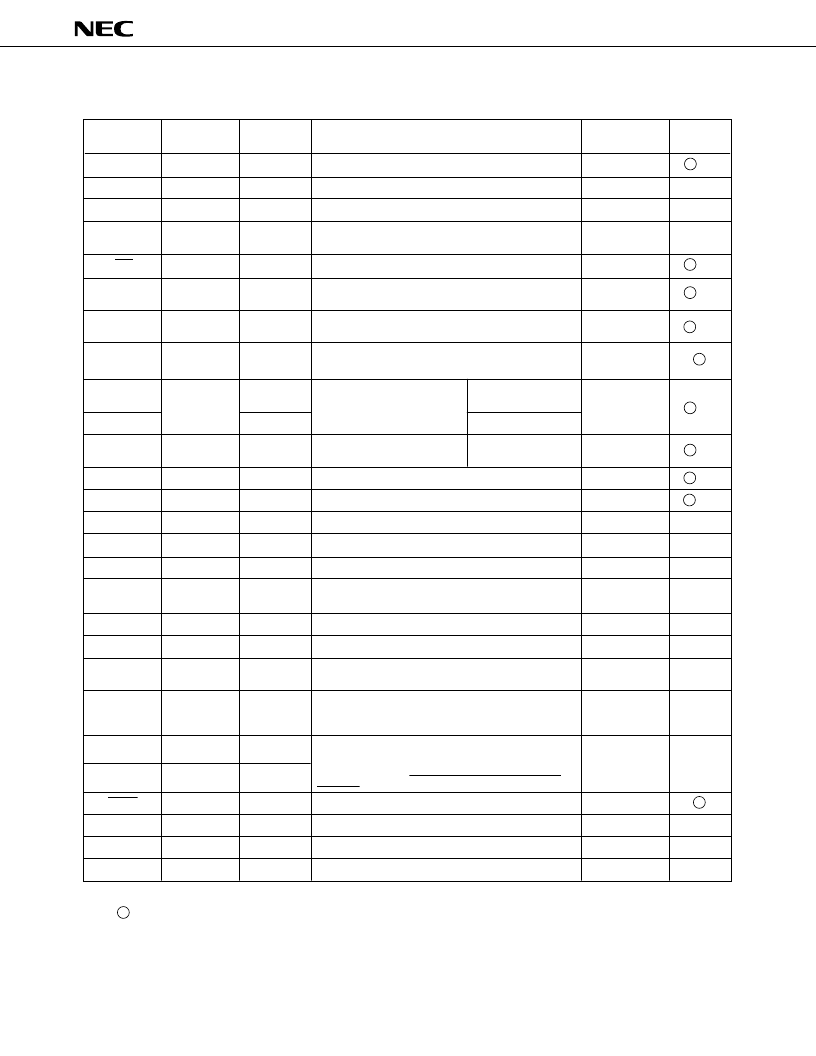
XT1
XT2
RESET
NC
*5
V
DD
V
SS
Function
External event pulse input pin to timer/event counter
Timer/event counter output pin
Clock output pin
Fixed frequency output pin (for buzzer or system clock
trimming)
Serial clock input/output pin
Serial data output pin
Serial bus input/output pin
Serial data input pin
Serial bus input/output pin
Edge detection vectored interrupt input pin (both rising
edge and falling edge detection effective)
Edge detection vectored
interrupt input pin (detection
edge selectable)
Edge detection testable input
pin (rising edge detection)
Parallel falling edge detection testable input pin
Parallel falling edge detection testable input pin
Segment signal output pin
Segment signal output pin
Common signal output pin
LCD drive power supply pin
On-chip split resistor (mask option)
External split resistor cut output pin
External expansion driver drive clock output pin
External expansion driver synchronization clock output
pin
Main system clock oscillation crystal/ceramic connection
pin. For external clock, the external clock signal is input
to X1 and its opposite phase is input to X2.
Subsystem clock oscillation crystal connection pin. For
external clock, the external clock signal is input to XT1
and XT2 is opened. XT1 can be used as a 1-bit input
(test) pin.
System reset input pin
NO CONNECTION
Positive power supply pin
GND potential pin
Pin Name
TI0
PTO0
PCL
BUZ
SCK
SO/SB0
SI/SB1
INT4
INT0
INT1
INT2
KR0 to KR3
KR4 to KR7
S0 to S23
S24 to S31
COM0 to COM3
V
LC0
to V
LC2
BIAS
LCDCL
*4
3.2
NON-PORT PINS
Dual-
Function Pin
P13
P20
P22
P23
P01
P02
P03
P00
P10
P11
P12
P60 to P63
P70 to P73
—
BP0 to BP7
—
—
—
P30
P31
—
—
—
—
—
—
—
Clock synchronous
system
Asynchronous
Asynchronous
*
1.
2.
Display outputs are selected with V
LCX
shown below as the input source.
S0 to S31: V
LC1
, COM0 to COM2: V
LC2
, COM3: V
LC0
: Schmitt trigger input
However, the level of each display output depends on the display output and V
LCX
external circuit.
Input/Output
Input
Input/output
Input/output
Input/output
Input/output
Input/output
Input/output
Input
Input
Input
Input/output
Input/output
Output
Output
Output
—
Output
Input/output
Input/output
Input
Input
—
Input
—
—
—
Input
Input
Input
Input
Input
Input
Input
Input
Input
Input
Input
Input
*2
*2
*2
—
*3
Input
Input
—
—
—
—
—
—
SYNC
*4
X1, X2
After
Reset
I/O Circuit
Type
*1
B - C
E - B
E - B
E - B
F - A
F - B
M - C
B
B - C
B - C
F - A
F - A
G - A
G - C
G - B
—
—
E - B
E - B
—
—
B
—
—
—
相關(guān)PDF資料 |
PDF描述 |
|---|---|
| UPD75306 | 4-Bit, Single-Chip Microcontrollers With LCD Controller/Driver |
| UPD75308 | 4-Bit, Single-Chip Microcontrollers With LCD Controller/Driver |
| UPD7554ACSA | 4-BIT SINGLE-CHIP MICROCOMPUTER |
| UPD7554AGA | 4-BIT SINGLE-CHIP MICROCOMPUTER |
| UPD7554A | 4-BIT SINGLE-CHIP MICROCOMPUTER |
相關(guān)代理商/技術(shù)參數(shù) |
參數(shù)描述 |
|---|---|
| UPD75306G182 | 制造商:Panasonic Industrial Company 功能描述:IC |
| UPD75308F478 | 制造商:Panasonic Industrial Company 功能描述:IC |
| UPD75308G699 | 制造商:Panasonic Industrial Company 功能描述:IC |
| UPD753204013 | 制造商:Panasonic Industrial Company 功能描述:IC |
| UPD7554AG-597-E2 | 制造商:Renesas Electronics Corporation 功能描述: |
發(fā)布緊急采購,3分鐘左右您將得到回復(fù)。