- 您現(xiàn)在的位置:買賣IC網(wǎng) > PDF目錄378747 > UPD75312GF (NEC Corp.) 4-BIT SINGLE-CHIP MICROCOMPUTER PDF資料下載
參數(shù)資料
| 型號: | UPD75312GF |
| 廠商: | NEC Corp. |
| 英文描述: | 4-BIT SINGLE-CHIP MICROCOMPUTER |
| 中文描述: | 4位單片機 |
| 文件頁數(shù): | 3/62頁 |
| 文件大?。?/td> | 577K |
| 代理商: | UPD75312GF |
第1頁第2頁當前第3頁第4頁第5頁第6頁第7頁第8頁第9頁第10頁第11頁第12頁第13頁第14頁第15頁第16頁第17頁第18頁第19頁第20頁第21頁第22頁第23頁第24頁第25頁第26頁第27頁第28頁第29頁第30頁第31頁第32頁第33頁第34頁第35頁第36頁第37頁第38頁第39頁第40頁第41頁第42頁第43頁第44頁第45頁第46頁第47頁第48頁第49頁第50頁第51頁第52頁第53頁第54頁第55頁第56頁第57頁第58頁第59頁第60頁第61頁第62頁
μ
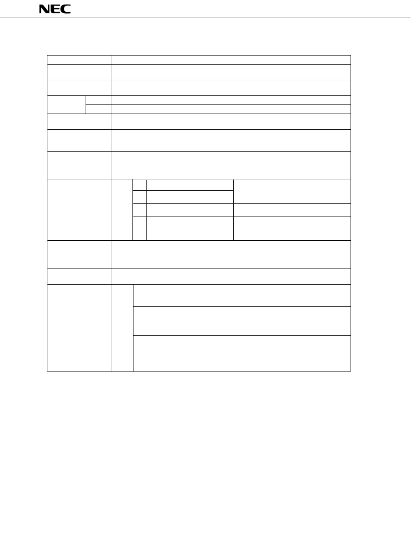
PD75312(A), 75316(A)
3
FUNCTIONAL OUTLINE (1/2)
Item
Function
Number of Basic
Instructions
Instruction Cycle
41
0.95
μ
s, 1.91
μ
s, 15.3
μ
s (Main system clock: operating at 4.19 MHz)
122
μ
s (Subsystem clock: operating at 32.768 kHz)
16256
×
8-bit (
μ
PD75316(A)), 12160
×
8-bit (
μ
PD75312(A))
512
×
4 bits
4-bit manipulation: 8 (B, C, D, E, H, L, X, A)
8-bit manipulation: 4
(
BC, DE, HL, XA)
Bit accumulator (CY)
4-bit accumulator (A)
8-bit accumulator (XA)
ROM
RAM
General-Purpose
Registers
Accumulator
Instruction Set
Abundant bit manipulation instructions
Efficient 4-bit data manipulation instructions
8-bit data transfer instructions
GETI instruction executing 2-/3-byte instruction with a single byte
40
8
CMOS input pins
I/O Line
Pull-up by software is possible.
: 23
16
CMOS input/output pins
8
CMOS output pins
Also serve as segment pins
8
N-ch open-drain input/output
Withstand voltage: 10 V
Pull-up by mask option is possible.
: 8
LCD Controller/
Driver
Segment number selection: 24/28/32 segments
(4/8 pins can also be used as bit ports.)
Display mode selection: Static, 1/2 duty, 1/3 duty (1/2 bias), 1/3 duty (1/3 bias), 1/4 duty
Dividing resistor for LCD driving can be built-in by mask option.
V
DD
= 2.7 to 6.0 V
Supply Voltage
Range
Internal
Memory
Timer
3 chs
8-bit timer/event counter
Clock source: 4 steps
Event count is possible
8-bit basic interval timer
Reference time generation: 1.95 ms, 7.82 ms, 31.3 ms, 250 ms
(operating at 4.19 MHz)
Can be used as watchdog timer
Watch timer
Generates 0.5-second time intervals
Count clock source: Main system clock or subsystem clock (selectable)
Watch fast forward mode (generates 3.9-ms time intervals)
Buzzer output (2 kHz)
相關(guān)PDF資料 |
PDF描述 |
|---|---|
| UPD75312GFA | 4-BIT SINGLE-CHIP MICROCOMPUTER |
| UPD75312A | 4-BIT SINGLE-CHIP MICROCOMPUTER |
| UPD75316 | 4-BIT SINGLE-CHIP MICROCOMPUTER |
| UPD75316A | 4-BIT SINGLE-CHIP MICROCOMPUTER |
| UPD75316GF | 4-BIT SINGLE-CHIP MICROCOMPUTER |
相關(guān)代理商/技術(shù)參數(shù) |
參數(shù)描述 |
|---|---|
| UPD753204013 | 制造商:Panasonic Industrial Company 功能描述:IC |
| UPD7554AG-597-E2 | 制造商:Renesas Electronics Corporation 功能描述: |
| UPD7554AG-597-E2-A | 制造商:Renesas Electronics Corporation 功能描述: |
| UPD7554AG-603-E2 | 制造商:Renesas Electronics Corporation 功能描述: |
| UPD7554AG-603-E2-A | 制造商:Renesas Electronics Corporation 功能描述: |
發(fā)布緊急采購,3分鐘左右您將得到回復(fù)。