- 您現(xiàn)在的位置:買賣IC網(wǎng) > PDF目錄378747 > UPD75312GF (NEC Corp.) 4-BIT SINGLE-CHIP MICROCOMPUTER PDF資料下載
參數(shù)資料
| 型號: | UPD75312GF |
| 廠商: | NEC Corp. |
| 英文描述: | 4-BIT SINGLE-CHIP MICROCOMPUTER |
| 中文描述: | 4位單片機(jī) |
| 文件頁數(shù): | 34/62頁 |
| 文件大?。?/td> | 577K |
| 代理商: | UPD75312GF |
第1頁第2頁第3頁第4頁第5頁第6頁第7頁第8頁第9頁第10頁第11頁第12頁第13頁第14頁第15頁第16頁第17頁第18頁第19頁第20頁第21頁第22頁第23頁第24頁第25頁第26頁第27頁第28頁第29頁第30頁第31頁第32頁第33頁當(dāng)前第34頁第35頁第36頁第37頁第38頁第39頁第40頁第41頁第42頁第43頁第44頁第45頁第46頁第47頁第48頁第49頁第50頁第51頁第52頁第53頁第54頁第55頁第56頁第57頁第58頁第59頁第60頁第61頁第62頁
μ
PD75312(A), 75316(A)
34
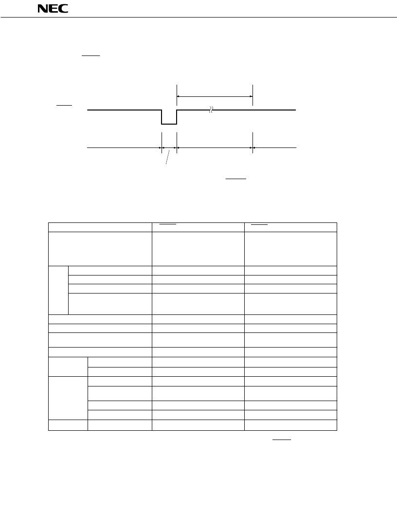
8. RESET FUNCTION
When the RESET signal is input, the
μ
PD75316(A) is reset and each hardware is initialized as indicated in
Table 8-1. Fig. 8-1 shows the reset operation timing.
RESET input
Wait
(31.3ms/4.19MHz)
Operation mode
or standby mode
HALT mode
Operation mode
Internal reset operation
Fig. 8-1 Reset Operation by RESET Input
Hardware
RESET Input in Standby Mode
RESET Input during Operation
Program Counter (PC)
The contents of the lower 6 bits
of address 0000H of the program
memory are set to PC13-8, and
the contents of address 0001H
are set to PC7-0.
The contents of the lower 6 bits
of address 0000H of the program
memory are set to PC13-8, and
the contents of address 0001H
are set to PC7-0.
PSW
Carry Flag (CY)
Retained
Undefined
Skip Flag (SK0-2)
0
0
Interrupt Status Flag (IST0)
0
0
Bank Enable Flag (MBE)
The contents of bit 7 of address
0000H of the program memory
are set to MBE.
The contents of bit 7 of address
0000H of the program memory
are set to MBE.
Stack Pointer (SP)
Undefined
Undefined
Data Memory (RAM)
General-Purpose Register
(X, A, H, L, D, E, B, C)
Retained *
Retained
Undefined
Undefined
Bank Selection Register (MBS)
0
0
Basic Interval
Timer
Counter (BT)
Undefined
Undefined
Timer/Event
Counter
Counter (T0)
0
0
Module Register
(TMOD0)
Mode Register (TM0)
FFH
FFH
0
0
TOE0, TOUT F/F
0, 0
0, 0
Mode Register (BTM)
0
0
Mode Register (WM)
0
Watch Timer
0
*
: Data of address 0F8H to 0FDH of the data memory becomes undefined when a RESET signal is input.
Table 8-1 Status of Each Hardware after Reset (1/2)
相關(guān)PDF資料 |
PDF描述 |
|---|---|
| UPD75312GFA | 4-BIT SINGLE-CHIP MICROCOMPUTER |
| UPD75312A | 4-BIT SINGLE-CHIP MICROCOMPUTER |
| UPD75316 | 4-BIT SINGLE-CHIP MICROCOMPUTER |
| UPD75316A | 4-BIT SINGLE-CHIP MICROCOMPUTER |
| UPD75316GF | 4-BIT SINGLE-CHIP MICROCOMPUTER |
相關(guān)代理商/技術(shù)參數(shù) |
參數(shù)描述 |
|---|---|
| UPD753204013 | 制造商:Panasonic Industrial Company 功能描述:IC |
| UPD7554AG-597-E2 | 制造商:Renesas Electronics Corporation 功能描述: |
| UPD7554AG-597-E2-A | 制造商:Renesas Electronics Corporation 功能描述: |
| UPD7554AG-603-E2 | 制造商:Renesas Electronics Corporation 功能描述: |
| UPD7554AG-603-E2-A | 制造商:Renesas Electronics Corporation 功能描述: |
發(fā)布緊急采購,3分鐘左右您將得到回復(fù)。