- 您現(xiàn)在的位置:買賣IC網(wǎng) > PDF目錄378747 > UPD75316BGK (NEC Corp.) 4-BIT SINGLE-CHIP MICROCOMPUTER PDF資料下載
參數(shù)資料
| 型號: | UPD75316BGK |
| 廠商: | NEC Corp. |
| 英文描述: | 4-BIT SINGLE-CHIP MICROCOMPUTER |
| 中文描述: | 4位單片機 |
| 文件頁數(shù): | 73/77頁 |
| 文件大小: | 587K |
| 代理商: | UPD75316BGK |
第1頁第2頁第3頁第4頁第5頁第6頁第7頁第8頁第9頁第10頁第11頁第12頁第13頁第14頁第15頁第16頁第17頁第18頁第19頁第20頁第21頁第22頁第23頁第24頁第25頁第26頁第27頁第28頁第29頁第30頁第31頁第32頁第33頁第34頁第35頁第36頁第37頁第38頁第39頁第40頁第41頁第42頁第43頁第44頁第45頁第46頁第47頁第48頁第49頁第50頁第51頁第52頁第53頁第54頁第55頁第56頁第57頁第58頁第59頁第60頁第61頁第62頁第63頁第64頁第65頁第66頁第67頁第68頁第69頁第70頁第71頁第72頁當前第73頁第74頁第75頁第76頁第77頁
73
μ
PD75312B, 75316B
0.95
μ
s, 1.91
μ
s, 15.3
μ
s (main system clock:@ 4.19 MHz)
122
μ
s (subsystem clock:@ 32.768 kHz)
Pull-up resistor can be incorporated by software: 23
40
Used with segment pin
10-V withstand voltage, pull-up resistor
can be incorporated by mask option.
10-V withstand voltage
,
without pull-up resistor option
Common output: Static – 1/4 duty selected
Segment output: Max. 32
LCD drive split resistor can be incorporated
by mask option.
No LCD drive split resistor
2.0 V to V
DD
8-bit timer/event counter
8-bit basic interval timer
Watch timer
NEC standard serial bus interface (SBI)
Clocked serial interface
External: 3
Internal: 3
External: 1
Internal: 1
Φ
, 524 kHz, 262 kHz, 65.5 kHz (main system clock:@ 4.19 MHz)
2 kHz (main system clock:@ 4.19 MHz, or subsystem clock:@ 32.768 KHz)
80-pin plastic QFP
(14 x 20 mm)
80-pin plastic QFP
(14 x 14 mm)
80-pin plastic TQFP
(Fine pitch) (12 x 12 mm)
80-pin plastic QFP
(14 x 14 mm)
80-pin plastic TQFP
(Fine pitch)
(12 x 12 mm)
80-pin plastic QFP
(14 x 14 mm)
80-pin plastic TQFP
(Fine pitch)
(12 x 12 mm)
80-pin ceramic
WQFN
*
80-pin plastic QFP
(14 x 20 mm)
80-pin ceramic
WQFN
GF package
GC/GK package :
μ
PD75P316B
:
μ
PD75P316A
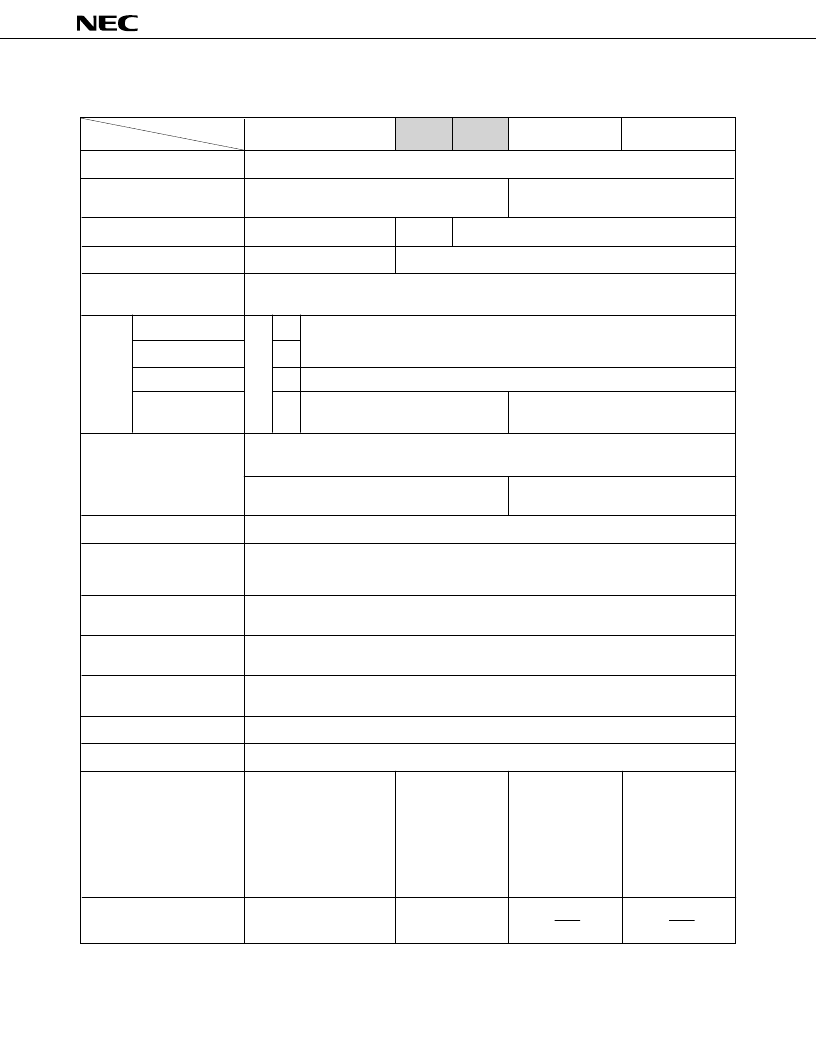
APPENDIX A. DIFFERENCES AMONG
μ
PD75308B SERIES PRODUCTS
Item
Supply voltage range
ROM configuration
Program memory (bytes)
Data memory (
×
4 bits)
Instruction cycle
CMOS input
CMOS input/output
CMOS output
N-ch open-drain
input/output
LCD controller/driver
LCD drive voltage
Timer/counter
Serial interface
Vectored interrupts
Test input
Clock output (PCL)
Buzzer output (BUZ)
Package
Name
μ
PD75P316A
μ
PD75P316B
μ
PD75304B/75306B/75308B
Mask ROM
4096/6016/8064
512
1024
Input/
output
port
8
16
8
8
μ
PD75312B
μ
PD75316B
2.0 to 6.0 V
12160
16256
EPROM/one-time PROM
*
Under development
μ
PD75P316B
On-chip PROM product
相關PDF資料 |
PDF描述 |
|---|---|
| UPD75312 | 4-BIT SINGLE-CHIP MICROCOMPUTER |
| UPD75316GFA | 4-BIT SINGLE-CHIP MICROCOMPUTER |
| UPD75312GF | 4-BIT SINGLE-CHIP MICROCOMPUTER |
| UPD75312GFA | 4-BIT SINGLE-CHIP MICROCOMPUTER |
| UPD75312A | 4-BIT SINGLE-CHIP MICROCOMPUTER |
相關代理商/技術(shù)參數(shù) |
參數(shù)描述 |
|---|---|
| UPD753204013 | 制造商:Panasonic Industrial Company 功能描述:IC |
| UPD7554AG-597-E2 | 制造商:Renesas Electronics Corporation 功能描述: |
| UPD7554AG-597-E2-A | 制造商:Renesas Electronics Corporation 功能描述: |
| UPD7554AG-603-E2 | 制造商:Renesas Electronics Corporation 功能描述: |
| UPD7554AG-603-E2-A | 制造商:Renesas Electronics Corporation 功能描述: |
發(fā)布緊急采購,3分鐘左右您將得到回復。