- 您現(xiàn)在的位置:買賣IC網(wǎng) > PDF目錄361647 > V370PDC-66 DRAM Controller PDF資料下載
參數(shù)資料
| 型號: | V370PDC-66 |
| 英文描述: | DRAM Controller |
| 中文描述: | DRAM控制器 |
| 文件頁數(shù): | 9/14頁 |
| 文件大?。?/td> | 205K |
| 代理商: | V370PDC-66 |
V370PDC
Copyright 1999, V3 Semiconductor Corp.
V370PDC_A0 Data Sheet Rev 1.00 DS-PD01-0100
9
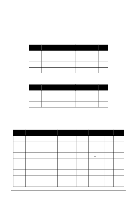
3.0 DC Specifications
The DC specifications for the PCI bus signals match exactly those given in the PCI Specification, Rev.
2.2 Section 4.2.1.1. For more information on the PCI DC specifications, see the PCI Specification.
3.1
PCI Bus DC Specifications
Table 5: Absolute Maximum Ratings
Symbol
Parameter
Value
Units
V
CC
Supply voltage
-0.3 to +3.6
V
V
IN
DC input voltage
-0.3 to 6.0
V
I
OUT
DC output current
TBA
mA
T
STG
Storage temperature range
-55 to +125
°C
Table 6: Guaranteed Operating Conditions
Symbol
Parameter
Value
Units
V
CC
Supply voltage
3.0 to 3.6
V
Theta Ja Thermal resistance
TBA
°C/w
T
A
Ambient temperature range
-40 to +85
°C
Table 7: PCI Bus Signals DC Operating Specifications
Symbol
Parameter
Condition
Min
Max
Units
Notes
V
IH
Input high voltage
0.5V
CC
V
CC
+ 0.5
V
V
IL
Input low voltage
-0.5
0.3V
CC
V
I
IH
Input high leakage current
0.7V
CC
μ
A
1
I
IL
Input low leakage current
0 < V
IN
< V
CC
+10
μ
A
1
V
OH
Output high voltage
I
OUT
= -500
μ
A
0.9V
CC
V
V
OL
Output low voltage
I
OUT
= 1500
μ
A
0.1V
CC
V
2
C
IN
Input pin capacitance
10
pF
3
C
CLK
PCLK pin capacitance
5
12
pF
C
IDSEL
IDSEL pin capacitance
8
pF
4
相關(guān)PDF資料 |
PDF描述 |
|---|---|
| V375A12M300A2L | Analog IC |
| V375A12M300A3 | Analog IC |
| V375A12M300A3L | Analog IC |
| V375A12M300AL | Analog IC |
| V375A12T300A2 | Analog IC |
相關(guān)代理商/技術(shù)參數(shù) |
參數(shù)描述 |
|---|---|
| V370PDC-66LP | 制造商:Rochester Electronics LLC 功能描述: 制造商:QuickLogic Corporation 功能描述: |
| V371 | 制造商:Varta 功能描述:Bulk |
| V3712PH | 制造商:Vishay Intertechnologies 功能描述: |
| V371AC | 制造商:Velleman Inc 功能描述: |
| V373 | 制造商:VARTA 功能描述: |
發(fā)布緊急采購,3分鐘左右您將得到回復(fù)。
