- 您現(xiàn)在的位置:買(mǎi)賣IC網(wǎng) > PDF目錄202173 > V59C1512808QAUF19 (PROMOS TECHNOLOGIES INC) 64M X 8 DDR DRAM, PBGA68 PDF資料下載
參數(shù)資料
| 型號(hào): | V59C1512808QAUF19 |
| 廠商: | PROMOS TECHNOLOGIES INC |
| 元件分類: | DRAM |
| 英文描述: | 64M X 8 DDR DRAM, PBGA68 |
| 封裝: | ROHS COMPLIANT, FBGA-68 |
| 文件頁(yè)數(shù): | 57/79頁(yè) |
| 文件大小: | 1028K |
| 代理商: | V59C1512808QAUF19 |
第1頁(yè)第2頁(yè)第3頁(yè)第4頁(yè)第5頁(yè)第6頁(yè)第7頁(yè)第8頁(yè)第9頁(yè)第10頁(yè)第11頁(yè)第12頁(yè)第13頁(yè)第14頁(yè)第15頁(yè)第16頁(yè)第17頁(yè)第18頁(yè)第19頁(yè)第20頁(yè)第21頁(yè)第22頁(yè)第23頁(yè)第24頁(yè)第25頁(yè)第26頁(yè)第27頁(yè)第28頁(yè)第29頁(yè)第30頁(yè)第31頁(yè)第32頁(yè)第33頁(yè)第34頁(yè)第35頁(yè)第36頁(yè)第37頁(yè)第38頁(yè)第39頁(yè)第40頁(yè)第41頁(yè)第42頁(yè)第43頁(yè)第44頁(yè)第45頁(yè)第46頁(yè)第47頁(yè)第48頁(yè)第49頁(yè)第50頁(yè)第51頁(yè)第52頁(yè)第53頁(yè)第54頁(yè)第55頁(yè)第56頁(yè)當(dāng)前第57頁(yè)第58頁(yè)第59頁(yè)第60頁(yè)第61頁(yè)第62頁(yè)第63頁(yè)第64頁(yè)第65頁(yè)第66頁(yè)第67頁(yè)第68頁(yè)第69頁(yè)第70頁(yè)第71頁(yè)第72頁(yè)第73頁(yè)第74頁(yè)第75頁(yè)第76頁(yè)第77頁(yè)第78頁(yè)第79頁(yè)
60
V59C1G01(408/808/168)QA Rev. 1.3 June 2008
ProMOS TECHNOLOGIES
V59C1G01(408/808/168)QA
Power and ground clamps are required on the following input only pins:
a) BA0-BAx
b) A0-Axx
c) RAS
d) CAS
e) WE
f) CS
g) ODT
h) CKE
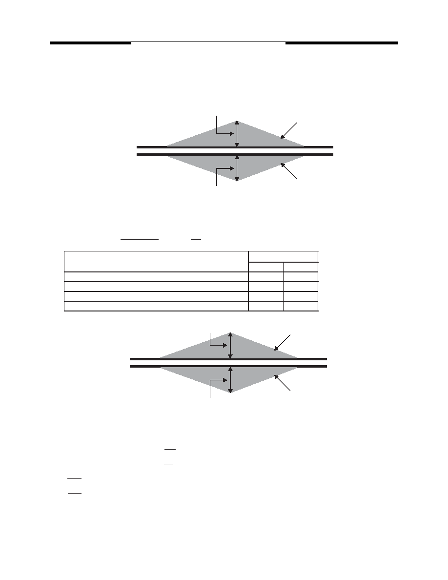
AC overshoot/undershoot specification for clock, data, strobe, and mask pins:
DQ, (U/L/R)DQS, (U/L/R)DQS, DM, CK, CK
Parameter
Specification
DDR2-667
DDR2-800
Maximum peak amplitude allowed for overshoot area (See Figure 75):
0.5 V
Maximum peak amplitude allowed for undershoot area (See Figure 75):
0.5 V
Maximum overshoot area above VDDQ (See Figure 75).
0.23 V-ns
Maximum undershoot area below VSSQ (See Figure 75).
0.23 V-ns
Overshoot Area
Maximum Amplitude
VDD
Undershoot Area
Maximum Amplitude
VSS
Volts
(V)
Time (ns)
AC overshoot and undershoot definition for address and control pins
Overshoot Area
Maximum Amplitude
VDDQ
Undershoot Area
Maximum Amplitude
VSSQ
Volts
(V)
Time (ns)
AC overshoot and undershoot definition for clock, data, strobe, and mask pins
AC & DC operating conditions (cont'd)
相關(guān)PDF資料 |
PDF描述 |
|---|---|
| V59C1512808QAUF5H | 64M X 8 DDR DRAM, PBGA68 |
| V59C1512804QALJ-37 | 64M X 8 DDR DRAM, 0.5 ns, PBGA68 |
| V59C1512164QAUJ19AI | 32M X 16 DDR DRAM, PBGA92 |
| V59C1512164QAUJ3 | 32M X 16 DDR DRAM, PBGA92 |
| V59C1512168QALF19A | 32M X 16 DDR DRAM, PBGA92 |
相關(guān)代理商/技術(shù)參數(shù) |
參數(shù)描述 |
|---|---|
| V5A010CB | 制造商:Honeywell Sensing and Control 功能描述:MICROSWITCH V5 PIN PLUNGER |
| V5A010CB | 制造商:Honeywell Sensing and Control 功能描述:MICROSWITCH V5 PIN PLUNGER |
| V5A010CB4D | 制造商:Honeywell Sensing and Control 功能描述:MICROSWITCH V5 ROLLER LEVER |
| V5A010CB4D | 制造商:Honeywell Sensing and Control 功能描述:MICROSWITCH V5 ROLLER LEVER |
| V5A010CB4E | 制造商:Honeywell Sensing and Control 功能描述:MICROSWITCH V5 ROLLER LEVER |
發(fā)布緊急采購(gòu),3分鐘左右您將得到回復(fù)。