- 您現(xiàn)在的位置:買賣IC網(wǎng) > PDF目錄203626 > W3E16M72S-266BI (WHITE ELECTRONIC DESIGNS CORP) 16M X 72 DDR DRAM, 0.75 ns, PBGA219 PDF資料下載
參數(shù)資料
| 型號: | W3E16M72S-266BI |
| 廠商: | WHITE ELECTRONIC DESIGNS CORP |
| 元件分類: | DRAM |
| 英文描述: | 16M X 72 DDR DRAM, 0.75 ns, PBGA219 |
| 封裝: | 32 X 25 MM, PLASTIC, BGA-219 |
| 文件頁數(shù): | 1/17頁 |
| 文件大?。?/td> | 766K |
| 代理商: | W3E16M72S-266BI |
1
White Electronic Designs Corporation (602) 437-1520 www.whiteedc.com
White Electronic Designs
W3E16M72S-XBX
February 2005
Rev. 7
GENERAL DESCRIPTION
The 128MByte (1Gb) DDR SDRAM is a high-speed CMOS,
dynamic random-access, memory using 5 chips containing
268,435,456 bits. Each chip is internally congured as a
quad-bank DRAM. Each of the chip’s 67,108,864-bit banks
is organized as 8,192 rows by 512 columns by 16 bits.
The 128 MB DDR SDRAM uses a double data rate
architecture to achieve high-speed operation. The
double data rate architecture is essentially a 2n-prefetch
architecture with an interface designed to transfer two data
words per clock cycle at the I/O pins. A single read or write
access for the 128MB DDR SDRAM effectively consists
of a single 2n-bit wide, one-clock-cycle data tansfer at the
internal DRAM core and two corresponding n-bit wide,
one-half-clock-cycle data transfers at the I/O pins.
A bidirectional data strobe (DQS) is transmitted externally,
16Mx72 DDR SDRAM
FEATURES
DDR SDRAM Rate = 200, 250, 266
Package:
219 Plastic Ball Grid Array (PBGA), 32 x 25mm
2.5V ±0.2V core power supply
2.5V I/O (SSTL_2 compatible)
Differential clock inputs (CLK and CLK#)
Commands entered on each positive CLK edge
Internal pipelined double-data-rate (DDR)
architecture; two data accesses per clock cycle
Programmable Burst length: 2,4 or 8
Bidirectional data strobe (DQS) transmitted/received
with data, i.e., source-synchronous data capture
(one per byte)
DQS edge-aligned with data for READs; center-
aligned with data for WRITEs
DLL to align DQ and DQS transitions with CLK
Four internal banks for concurrent operation
Two data mask (DM) pins for masking write data
Programmable IOL/IOH option
Auto precharge option
Auto Refresh and Self Refresh Modes
Commercial, Industrial and Military Temperature
Ranges
Organized as 16M x 72
Weight: W3E16M72S-XBX – 3.55 grams typical
* This product is subject to change without notice..
BENEFITS
40% SPACE SAVINGS
Reduced part count
Reduced I/O count
34% I/O Reduction
Reduced trace lengths for lower parasitic
capacitance
Suitable for hi-reliability applications
Laminate interposer for optimum TCE match
Upgradeable to 32M x 72 density
(W3E32M72S-XBX)
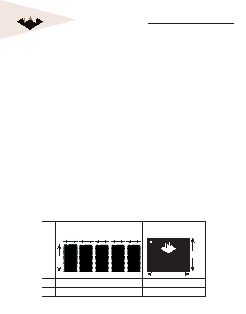
25
32
66
TSOP
66
TSOP
66
TSOP
66
TSOP
11.9
22.3
Monolithic Solution
Actual Size
W3E16M72S-XBX
S
A
V
I
N
G
S
Area
I/O
Count
5 x 265mm2 = 1328mm2
5 x 66 pins = 330 pins
800mm2
40%
219 Balls
34%
W3E16M72S-XBX
White Electronic Designs
相關PDF資料 |
PDF描述 |
|---|---|
| W3E16M72S-200BI | 16M X 72 DDR DRAM, 0.8 ns, PBGA219 |
| W3E16M72SR-200BM | 16M X 72 DDR DRAM, 0.75 ns, PBGA219 |
| W3E16M72SR-200BC | 16M X 72 DDR DRAM, 0.75 ns, PBGA219 |
| W3E16M72SR-200BM | 16M X 72 DDR DRAM, 0.75 ns, PBGA219 |
| W3EG2128M72AFSR262AD3M | 256M X 72 DDR DRAM MODULE, 0.75 ns, DMA184 |
相關代理商/技術參數(shù) |
參數(shù)描述 |
|---|---|
| W3E16M72S-266BM | 制造商:Microsemi Corporation 功能描述:16M X 72 DDR, 2.5V, 266 MHZ, 219 PBGA, MIL-TEMP. - Bulk |
| W3E16M72S-333BC | 制造商:Microsemi Corporation 功能描述:16M X 72 DDR, 2.5V, 333 MHZ, 219 PBGA, COMMERCIAL TEMP. - Bulk |
| W3E16M72S-333BI | 制造商:Microsemi Corporation 功能描述:16M X 72 DDR, 2.5V, 333 MHZ, 219 PBGA, INDUSTRIAL TEMP. - Bulk |
| W3E16M72S-333BM | 制造商:Microsemi Corporation 功能描述:16M X 72 DDR, 2.5V, 333 MHZ, 219 PBGA, MIL-TEMP. - Bulk |
| W3E16M72SR-200BC | 制造商:WEDC 制造商全稱:White Electronic Designs Corporation 功能描述:16Mx72 Registered DDR SDRAM |
發(fā)布緊急采購,3分鐘左右您將得到回復。