- 您現(xiàn)在的位置:買(mǎi)賣(mài)IC網(wǎng) > PDF目錄202126 > W3HG232M64SEU806D4GG (MICROSEMI CORP-PMG MICROELECTRONICS) 64M X 64 DDR DRAM MODULE, 0.4 ns, DMA200 PDF資料下載
參數(shù)資料
| 型號(hào): | W3HG232M64SEU806D4GG |
| 廠商: | MICROSEMI CORP-PMG MICROELECTRONICS |
| 元件分類(lèi): | DRAM |
| 英文描述: | 64M X 64 DDR DRAM MODULE, 0.4 ns, DMA200 |
| 封裝: | ROHS COMPLIANT, SO-DIMM-200 |
| 文件頁(yè)數(shù): | 13/13頁(yè) |
| 文件大小: | 154K |
| 代理商: | W3HG232M64SEU806D4GG |
第1頁(yè)第2頁(yè)第3頁(yè)第4頁(yè)第5頁(yè)第6頁(yè)第7頁(yè)第8頁(yè)第9頁(yè)第10頁(yè)第11頁(yè)第12頁(yè)當(dāng)前第13頁(yè)
W3HG232M64SEU-D4
June 2007
Rev. 2
ADVANCED
9
White Electronic Designs Corporation (602) 437-1520 www.whiteedc.com
White Electronic Designs
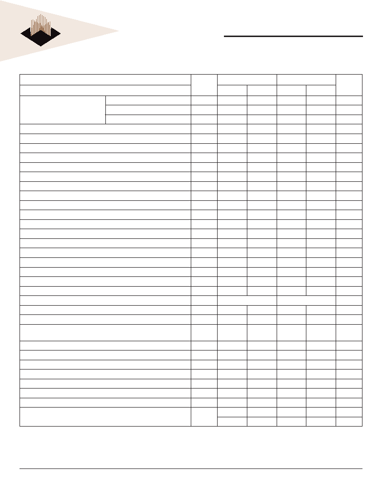
COMPONENTS AC OPERATING CONDITIONS
AC Characteristics
Symbol
534
403
Units
Parameter
Min
Max
Min
Max
Clock Frequency
CL = 3
tCK
5858
ns
CL = 4
tCK
3.75
8
5
8
ns
CL = 5
tCK
3.75
8
5
8
ns
DQ output access time from CK / CK
tAC
-500
+500
-600
+600
ps
CAS A to CAS B command period
tCCD
2-2-
tCK
CK, CK high-level width
tCH
0.45
0.55
0.45
0.55
tCK
CKE minimum high and low pulse width
tCKE
3-3-
tCK
CK, CK low-level width
tCL
0.45
0.55
0.45
0.55
tCK
Auto-Precharge write recovery + precharge time
tDAL
WR + tRP
-
WR + tRP
-tCK
Minimum time clocks remain ON after CKE asynchronously drops LOW
DELAY
tIS + tCK + tIH
-tIS + tCK + tIH
-ns
DQ and DM input hold time (differential data strobe)
tDH(base)
225
-
275
-
ps
DQ and DM input hold time (single ended data strobe)
tDH1(base)
-25
-
-25
-
ps
DQ and DM input pulse width (each input)
DIPW
0.35
-
0.35
-
tCK
DQS output access time from CK / CK
tDQSCK
-450
+450
-500
+500
ps
DQS input low (high) pulse width (write cycle)
QSL,H
0.35
-
0.35
-
tCK
DQS-DQ skew (for DQS & associated DQ signals)
tDQSQ
-
300
-
350
ps
Write command to 1st DQS latching transition
tDQSS
-0.25
+0.25
-0.25
+0.25
tCK
DQ and DM input setup time (differential data strobe)
tDS(base)
100
-
150
-
ps
DQ and DM input setup time (single ended data strobe)
tDS1(base)
-25
-
-25
-
ps
DQS falling edge hold time from CK (write cycle)
tDSH
0.2
-
0.2
-
tCK
DQS falling edge to CK setup time (write cycle)
tDSS
0.2
-
0.2
-
tCK
Clock half period
tHP
MIN
. (tCL, tCH
MIN
. (tCL, tCH
-
Data-out high-impedance time from CK / CK
tHZ
-tAC.MAX
ps
Address and control input hold time
tIH(base)
375
-
475
-
ps
Address and control input pulse width
(each input)
tIPW
0.6
-
0.6
-
tCK
Address and control input setup time
tIS(base)
250
-
350
-
ps
DQ low-impedance time from CK / CK
tLZ(DQ)
2x tAC.MIN
tAC.MAX
2x tAC.MIN
tAC.MAX
ps
DQS low-impedance from CK / CK
tLZ(DQS)
tAC.MIN
tAC.MAX-
tAC.MIN
tAC.MAX-
ps
Mode register set command cycle time
tMRD
2-2-
tCK
OCD drive mode output delay
tOIT
012012
ns
Data output hold time from DQS
tQH
tHP –tQHS
-tHP –tQHS
-
Data hold skew factor
tQHS
-
400
-
450
ps
Average periodic refresh Interval
tREFI
-
7.8
-
7.8
-
3.9
-
3.9
s
Note:
AC specication is based on
QIMONDA components. Other DRAM manufactures specication may be different.
Continued on next page
相關(guān)PDF資料 |
PDF描述 |
|---|---|
| W3HG64M72EER403PD4MG | 64M X 72 DDR DRAM MODULE, 0.6 ns, DMA200 |
| W7NCF02GH20CS3AG | 128M X 16 FLASH 3.3V PROM CARD, 150 ns, UUC |
| W7NCF02GH20CS7JG | 128M X 16 FLASH 3.3V PROM CARD, 150 ns, UUC |
| W7NCF02GH20IS7CG | 128M X 16 FLASH 3.3V PROM CARD, 150 ns, UUC |
| W7NCF08GH10CSAAG | 512M X 16 FLASH 3.3V PROM CARD, 150 ns, UUC |
相關(guān)代理商/技術(shù)參數(shù) |
參數(shù)描述 |
|---|---|
| W3HG264M72EER403AD7XG | 制造商:WEDC 制造商全稱(chēng):White Electronic Designs Corporation 功能描述:1GB - 2x64Mx72 DDR2 SDRAM REGISTERED, w/PLL, VLP Mini-DIMM |
| W3HG264M72EER534AD7XG | 制造商:WEDC 制造商全稱(chēng):White Electronic Designs Corporation 功能描述:1GB - 2x64Mx72 DDR2 SDRAM REGISTERED, w/PLL, VLP Mini-DIMM |
| W3HG264M72EER665AD7XG | 制造商:WEDC 制造商全稱(chēng):White Electronic Designs Corporation 功能描述:1GB - 2x64Mx72 DDR2 SDRAM REGISTERED, w/PLL, VLP Mini-DIMM |
| W3HG264M72EER806AD7XG | 制造商:WEDC 制造商全稱(chēng):White Electronic Designs Corporation 功能描述:1GB - 2x64Mx72 DDR2 SDRAM REGISTERED, w/PLL, VLP Mini-DIMM |
| W3HG264M72EER-AD7 | 制造商:WEDC 制造商全稱(chēng):White Electronic Designs Corporation 功能描述:1GB - 2x64Mx72 DDR2 SDRAM REGISTERED, w/PLL, VLP Mini-DIMM |
發(fā)布緊急采購(gòu),3分鐘左右您將得到回復(fù)。