- 您現(xiàn)在的位置:買(mǎi)賣(mài)IC網(wǎng) > PDF目錄68459 > W6694ACD (WINBOND ELECTRONICS CORP) DATACOM, ISDN CONTROLLER, PQFP48 PDF資料下載
參數(shù)資料
| 型號(hào): | W6694ACD |
| 廠商: | WINBOND ELECTRONICS CORP |
| 元件分類(lèi): | 數(shù)字傳輸電路 |
| 英文描述: | DATACOM, ISDN CONTROLLER, PQFP48 |
| 封裝: | 7 X 7 MM, 1.40 MM HEIGHT, LQFP-48 |
| 文件頁(yè)數(shù): | 42/42頁(yè) |
| 文件大?。?/td> | 567K |
| 代理商: | W6694ACD |
第1頁(yè)第2頁(yè)第3頁(yè)第4頁(yè)第5頁(yè)第6頁(yè)第7頁(yè)第8頁(yè)第9頁(yè)第10頁(yè)第11頁(yè)第12頁(yè)第13頁(yè)第14頁(yè)第15頁(yè)第16頁(yè)第17頁(yè)第18頁(yè)第19頁(yè)第20頁(yè)第21頁(yè)第22頁(yè)第23頁(yè)第24頁(yè)第25頁(yè)第26頁(yè)第27頁(yè)第28頁(yè)第29頁(yè)第30頁(yè)第31頁(yè)第32頁(yè)第33頁(yè)第34頁(yè)第35頁(yè)第36頁(yè)第37頁(yè)第38頁(yè)第39頁(yè)第40頁(yè)第41頁(yè)當(dāng)前第42頁(yè)
Preliminary Data Sheet
W6694A USB-ISDN S/T-Controller
-9-
Publication Release Date: May, 2001
Revision 1.03
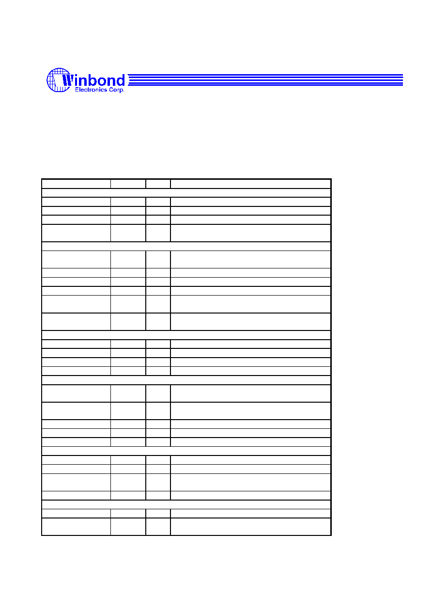
4. PIN DESCRIPTION
TABLE 4.1 PIN DESCRIPTIONS
Note: The suffix # indicates active LOW signal.
Symbol
Pin No.
I/O
Function
USB Bus
D+
38
I/O
USB D+ data line
D-
39
I/O
USB D- data line
UCLK1
41
I
24 MHz crystal/oscillator clock input
UCLK2
42
O
24 MHz crystal clock output. Left unconnected if
use oscillator.
ISDN Signals and External Crystal
SR1
45
I
S/T bus receiver input (-). This is normal polarity.
Reverse polarity is also OK.
SR2
46
I
S/T bus receiver input (+)
SX1
48
O
S/T bus transmitter output(+)
SX2
1
O
S/T bus transmitter output(-)
XTAL1
2
I
Crystal or Oscillator clock input. The clock
frequency: 7.68MHz
±100PPM.
XTAL2
3
O
Crystal clock output. Left unconnected when using
oscillator.
GCI Bus
GCIDCL
6
I
GCI bus data clock 1.536 MHz
GCIFSC
7
I
GCI bus frame synchronization clock
GCIDD
8
I
GCI bus data downstream (input)
GCIDU
9
O
GCI bus data upstream (output)
PCM Bus
PFCK1
10
O
PCM port 1 frame synchronization signal with 8
KHz repetition rate and 8 bit pulse width
PFCK2
11
O
PCM port 2 frame synchronization signal with 8
KHz repetition rate and 8 bit pulse width
PBCK
12
O
PCM bit clock of 1.536 MHz
PTXD
15
O
PCM data output
PRXD
16
I
PCM data input
External Serial EEPROM Interface
EPCS
17
O
Serial EEPROM chip select
EPSK
18
O
Serial EEPROM data clock
EPDI
19
I
Serial EEPROM data input. Internal 10k ohm pull-
up is provided.
EPDO
20
O
Serial EEPROM data output
Power and Ground
VDD1,VSS1
47,44
I
ISDN S/T analog power (5V), Ground
VDD21,VSS21
VDD22,VSS22
5,4
14,13
I
Digital power (5V), Ground
相關(guān)PDF資料 |
PDF描述 |
|---|---|
| W671320P | TELECOM-SLIC, PQCC28 |
| W671361P | TELECOM-SLIC, PQCC28 |
| W671361Y | TELECOM-SLIC, QCC32 |
| W671310P | TELECOM-SLIC, PQCC28 |
| W671340P | TELECOM-SLIC, PQCC28 |
相關(guān)代理商/技術(shù)參數(shù) |
參數(shù)描述 |
|---|---|
| W6694CD | 制造商:WINBOND 制造商全稱(chēng):Winbond 功能描述:USB Bus ISDN S/T-Controller |
| W66ARX-18 | 制造商:Magnecraft 功能描述: |
| W66MAF185X | 制造商:Panasonic Industrial Company 功能描述:CRT |
| W66R_1G WAF | 制造商:Fairchild Semiconductor Corporation 功能描述: |
| W66TX-25 | 制造商:Magnecraft 功能描述: |
發(fā)布緊急采購(gòu),3分鐘左右您將得到回復(fù)。