- 您現(xiàn)在的位置:買賣IC網(wǎng) > PDF目錄68747 > W9412FASA-75 (WINBOND ELECTRONICS CORP) 16M X 64 DDR DRAM MODULE, 0.75 ns, DMA200 PDF資料下載
參數(shù)資料
| 型號: | W9412FASA-75 |
| 廠商: | WINBOND ELECTRONICS CORP |
| 元件分類: | DRAM |
| 英文描述: | 16M X 64 DDR DRAM MODULE, 0.75 ns, DMA200 |
| 封裝: | SODIMM-200 |
| 文件頁數(shù): | 13/15頁 |
| 文件大小: | 0K |
| 代理商: | W9412FASA-75 |
W9412FASA
Publication Release Date: March 15, 2002
- 7 -
Revision A1
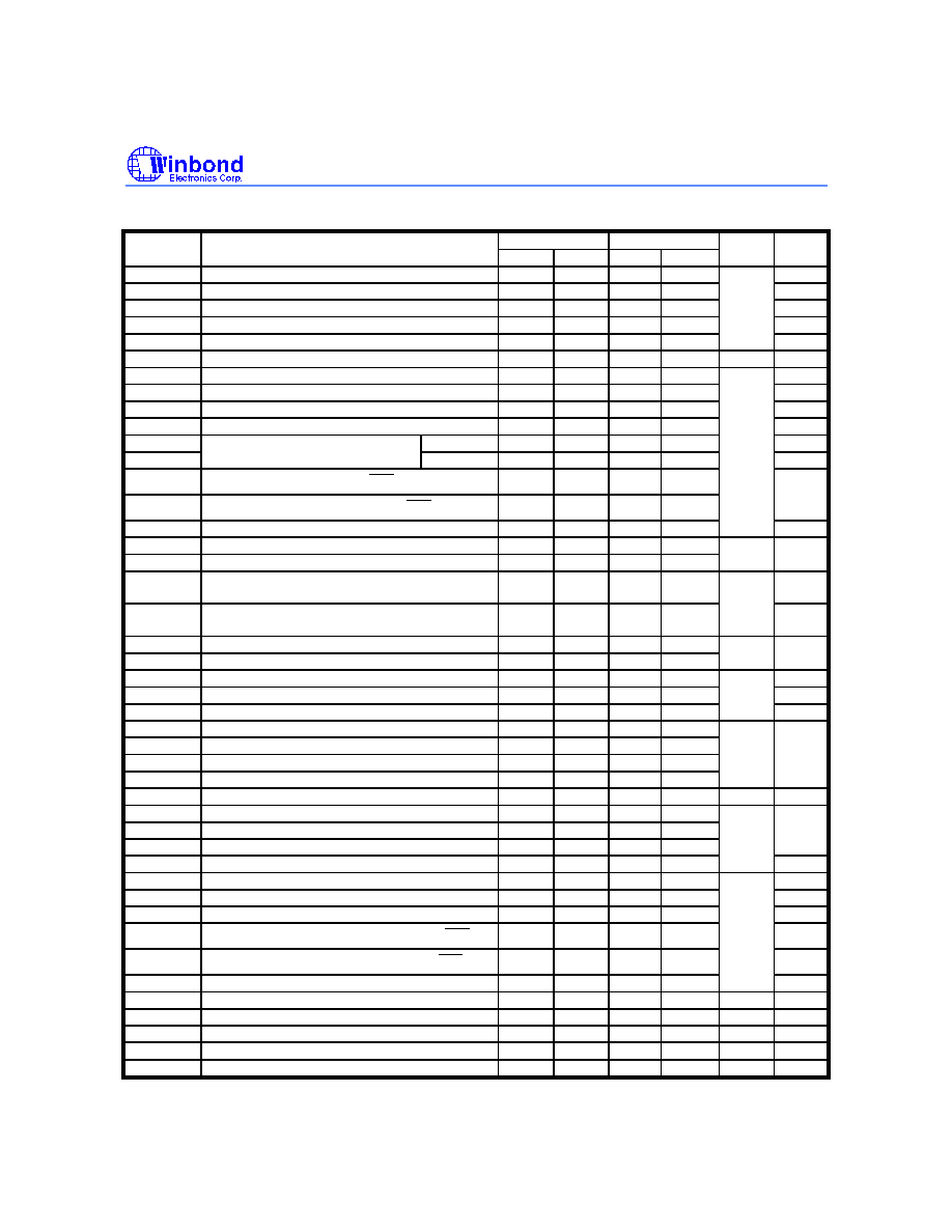
11. AC CHARACTERISTICS OF SDRAM COMPONENTS (Notes: 10, 12)
SYMBOL
PARAMETER
-7
-75
UNITS
NOTES
MIN.
MAX.
MIN.
MAX.
tRC
Active to Ref/Active Command Period
65
tRFC
Ref to Ref/Active Command Period
75
tRAS
Active to Precharge Command Period
45
100000
45
100000
tRCD
Active to Read/Write Command Delay Time
15
tRAP
Active to Read with Auto Precharge enable
15
nS
tCCD
Read/Write (a) to Read/Write (b) Command Period
1
tCK
tRP
Precharge to Active Command Period
20
tRRD
Active (a) to Active (b) Command Period
15
tWR
Write Recovery time
15
tDAL
Auto Precharge Write Recovery + Precharge time
30
tCK
CL = 2
7.5
15
8
15
CLK Cycle Time
CL = 2.5
7
15
7.5
15
tAC
Data Access time from CLK, CLK
-0.75
0.75
-0.75
0.75
tDQSCK
DQS output access time from CLK, CLK
-0.75
0.75
-0.75
0.75
16
tDQSQ
Data Strobe Edge to Output Data Edge Skew
0.5
ns
tCH
CLk High Level Width
0.45
0.55
0.45
0.55
tCL
CLK Low Level Width
0.45
0.55
0.45
0.55
tCK
11
tHP
CLK Half Period (minimum of actual tCH, tCL)
Min.
(tCL,tCH)
Min.
(tCL,tCH)
tQH
DQ Output Data Hold Time from DQS
tHP
-0.75
tHP
-0.75
nS
tRPRE
DQS Read Preamble Time
0.9
1.1
0.9
1.1
tRPST
DQS Read Postamble Time
0.4
0.6
0.4
0.6
tCK
11
tDS
DQ and DM Setup Time
0.5
tDH
DQ and DM Hold Time
0.5
tDIPW
DQ and DM Input Pulse Width (for each input)
1.75
nS
tDQSH
DQS Input High Pulse Width
0.35
tDQSL
DQS Input Low Pulse Width
0.35
tDSS
DQS Falling Edge to CLK Setup Time
0.2
tDSH
DQS Falling Edge Hold Time from CLK
0.2
tCK
11
tWPRES
Clock to DQS Write Preamble Set-up Time
0
nS
tWPRE
DQS Write Preamble Time
0.25
tWPST
DQS Write Postamble Time
0.4
tDQSS
Write Command to First DQS Latching Transition
0.75
1.25
0.75
1.25
11
tDSSK
UDQS – LDQS Skew (x 16)
-0.25
0.25
-0.25
0.25
tCK
tIS
Input Setup Time
0.9
tIH
Input Hold Time
0.9
tIPW
Control & Address Input Pulse Width (for each input)
2.2
tHZ
Data-out High-impedance Time from CLK, CLK
-0.75
0.75
-0.75
0.75
tLZ
Data-out Low-impedance Time from CLK, CLK
-0.75
0.75
-0.75
0.75
tT(SS)
SSTL Input Transition
0.5
1.5
0.5
1.5
nS
tWTR
Internal Write to Read Command Delay
1
tCK
tXSNR
Exit Self Refresh to Non-read Command
75
nS
tXSRD
Exit Self Refresh to Read Command
10
tCK
tREF
Refresh Time (8K)
64
mS
tMRD
Mode Register Set Cycle Time
15
nS
相關PDF資料 |
PDF描述 |
|---|---|
| W9425G6EH-6 | 16M X 16 DDR DRAM, 0.7 ns, PDSO66 |
| W9425G6EH-4 | 16M X 16 DDR DRAM, 0.7 ns, PDSO66 |
| W9864G6GB-6I | 4M X 16 SYNCHRONOUS DRAM, 5.5 ns, PBGA60 |
| WE256K32-250G2TMEA | 256K X 32 EEPROM 5V MODULE, 250 ns, CQFP68 |
| WE256K32-200G2TCE | 256K X 32 EEPROM 5V MODULE, 200 ns, CQFP68 |
相關代理商/技術參數(shù) |
參數(shù)描述 |
|---|---|
| W9412G2CB | 制造商:WINBOND 制造商全稱:Winbond 功能描述:1M 】 4 BANKS 】 32 BITS GDDR SDRAM |
| W9412G2IB | 制造商:WINBOND 制造商全稱:Winbond 功能描述:1M × 4 BANKS × 32 BITS GDDR SDRAM |
| W9412G2IB4 | 制造商:WINBOND 制造商全稱:Winbond 功能描述:Double Data Rate architecture; two data transfers per clock cycle |
| W9412G2IB-5 | 制造商:Winbond Electronics Corp 功能描述:8*16 DDR1 |
| W9412G6CH | 制造商:WINBOND 制造商全稱:Winbond 功能描述:2M 】 4 BANKS 】 16 BITS DDR SDRAM |
發(fā)布緊急采購,3分鐘左右您將得到回復。