- 您現(xiàn)在的位置:買(mǎi)賣(mài)IC網(wǎng) > PDF目錄361798 > W9451GBDA-6 SDRAM|DDR|64MX64|CMOS|DIMM|184PIN|PLASTIC PDF資料下載
參數(shù)資料
| 型號(hào): | W9451GBDA-6 |
| 英文描述: | SDRAM|DDR|64MX64|CMOS|DIMM|184PIN|PLASTIC |
| 中文描述: | 內(nèi)存|復(fù)員| 64MX64 |的CMOS |內(nèi)存| 184PIN |塑料 |
| 文件頁(yè)數(shù): | 3/15頁(yè) |
| 文件大小: | 284K |
| 代理商: | W9451GBDA-6 |
第1頁(yè)第2頁(yè)當(dāng)前第3頁(yè)第4頁(yè)第5頁(yè)第6頁(yè)第7頁(yè)第8頁(yè)第9頁(yè)第10頁(yè)第11頁(yè)第12頁(yè)第13頁(yè)第14頁(yè)第15頁(yè)
W9451GBDA-6
Publication Release Date: March 15, 2002
- 3 -
Revision A1
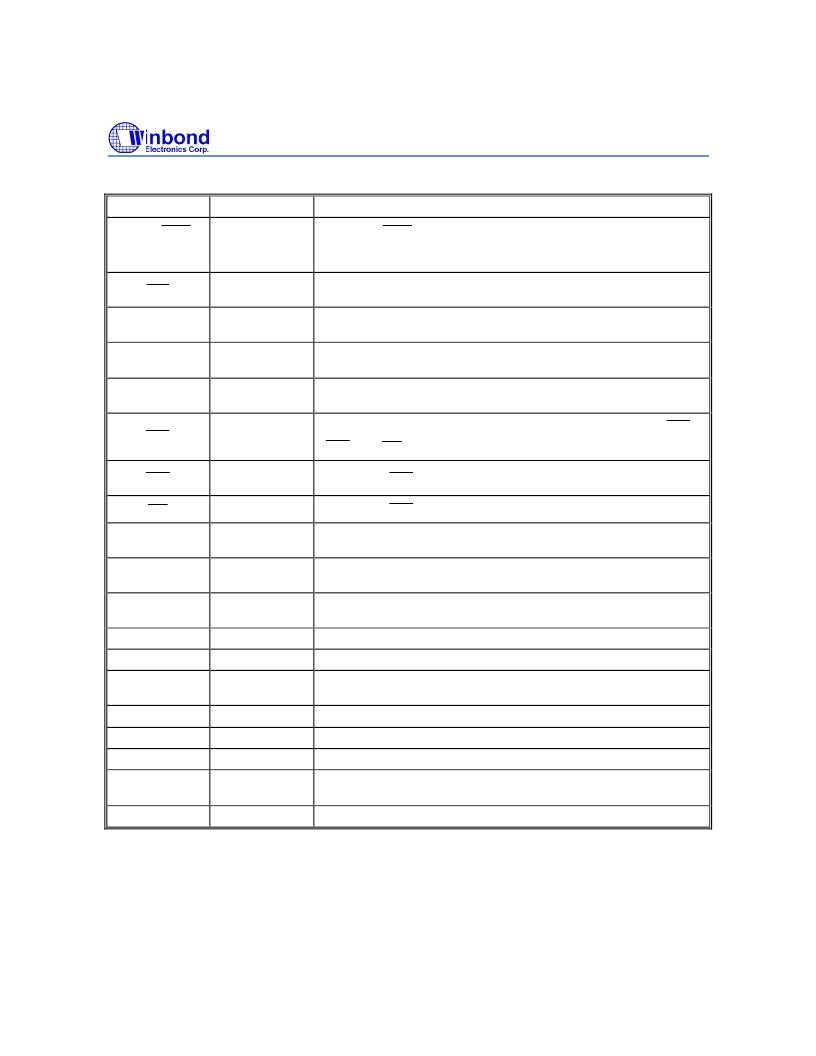
5. PIN DESCRIPTIONS
PIN
NAME
FUNCTION DESCRIPTION
CLKn, CLKn
Clock Input
CLKn and CLKn are differential clock inputs. All input command
signals are sampled at the positive edge of CLK(except for DQ, DM
and CKE).
CSn
Chip select
Disable or enable the command decoder. When command decoder is
disabled, new command is ignored and previous operation continues.
CKEn
Clock Enable
CKE controls the clock activation and deactivation. When CKE is low,
Power Down mode, Suspend mode, or Self-Refresh mode is entered.
A0
A12
Address
Multiplexed pins for row and column address.
Row address: A0
A12. Column address: A0
A9.
BA0
BA1
Bank Select
Address
Selects bank to be activated during row address latch time.
Selects bank for read/write during column address latch time.
RAS
Row Address
Strobe
Command input. When sampled at the rising edge of the clock, RAS ,
CAS and WE define the operation to be executed.
CAS
Column
Address Strobe
Referred to RAS
WE
Write Enable
Referred to RAS
DM0
DM7
Input/Output
Mask
The output buffer is placed at Hi-Z when DM is sampled high in read
cycle. In write cycle, sampling DM high will block the write data.
DQ0
DQ63
Data
Input/Output
Multiplexed pins for data output and input
DQS0
DQS7
Data Strobe
Input/Output
Output with read data, input with write data. DQS is edge-aligned with
read data, centered in write data.
V
DD
Power (+2.5V)
Power supply (2.5V).
V
SS
Ground
Ground
V
REF
Reference
Voltage
SSTL-2 Reference voltage
V
DDSPD
SPD Power
Separated power supply for SPD EEPROM (2.3V
3.6V)
SCL
Serial Clock
Clock for serial presence detection
SDA
Serial Data I/O
Data line for serial presence detection
SAn
SPD Address
Line
System assigned address (SA0
SA2) to identify different memory
module in a system board.
NC
No Connection
No connection
相關(guān)PDF資料 |
PDF描述 |
|---|---|
| W981204AH-75 | x4 SDRAM |
| W981204AH-8H | x4 SDRAM |
| W982504AH-7 | x4 SDRAM |
| W982504AH-75 | x4 SDRAM |
| W982504AH-8H | x4 SDRAM |
相關(guān)代理商/技術(shù)參數(shù) |
參數(shù)描述 |
|---|---|
| W946432AD | 制造商:WINBOND 制造商全稱(chēng):Winbond 功能描述:512K X 4 BANKS X 32 BITS DDR SDRAM |
| W9464G6IB | 制造商:WINBOND 制造商全稱(chēng):Winbond 功能描述:1M × 4 BANKS × 16 BITS DDR SDRAM |
| W9464G6IH | 制造商:WINBOND 制造商全稱(chēng):Winbond 功能描述:1M ?? 4 BANKS ?? 16 BITS DDR SDRAM |
| W9464G6JH | 制造商:WINBOND 制造商全稱(chēng):Winbond 功能描述:1M ? 4 BANKS ? 16 BITS DDR SDRAM |
| W9464G6JH-4 | 制造商:Winbond Electronics Corp 功能描述:IC DDR SDRAM 64M 200MHZ 66TSOP |
發(fā)布緊急采購(gòu),3分鐘左右您將得到回復(fù)。