- 您現(xiàn)在的位置:買賣IC網(wǎng) > PDF目錄140380 > WED9LC6416V1612BC SPECIALTY MEMORY CIRCUIT, PBGA153 PDF資料下載
參數(shù)資料
| 型號: | WED9LC6416V1612BC |
| 元件分類: | 存儲器 |
| 英文描述: | SPECIALTY MEMORY CIRCUIT, PBGA153 |
| 封裝: | MO-163, BGA-153 |
| 文件頁數(shù): | 26/27頁 |
| 文件大?。?/td> | 370K |
| 代理商: | WED9LC6416V1612BC |
第1頁第2頁第3頁第4頁第5頁第6頁第7頁第8頁第9頁第10頁第11頁第12頁第13頁第14頁第15頁第16頁第17頁第18頁第19頁第20頁第21頁第22頁第23頁第24頁第25頁當(dāng)前第26頁第27頁
8
White Electronic Designs Corporation (508) 366-5151 www.whiteedc.com
WED9LC6416V
January 2001
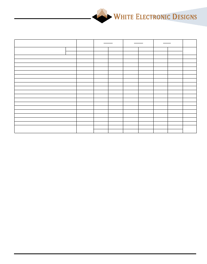
SDRAM AC CHARACTERISTICS
(VCC = 3.3V -5% / +10% unless otherwise noted; 0
°C ≤ TA ≤ 70°C, Commercial; -40°C ≤ TA ≤ 85°C, Industrial)
Symbol
125MHz
100MHz
83MHz
Parameter
Min
Max
Min
Max
Min
Max
Units
Clock Cycle Time (1)
CL = 3
tCC
8
1000
10
1000
12
1000
ns
CL = 2
tCC
10
1000
12
1000
15
1000
Clock to valid Output delay (1,2)
tSAC
67
8
ns
Output Data Hold Time (2)
tOH
33
3
ns
Clock HIGH Pulse Width (3)
tCH
33
3
ns
Clock LOW Pulse Width (3)
tCL
33
3
ns
Input Setup Time (3)
tSS
22
2
ns
Input Hold Time (3)
tSH
11
1
ns
CLK to Output Low-Z (2)
tSLZ
22
2
ns
CLK to Output High-Z
tSHZ
77
8
ns
Row Active to Row Active Delay (4)
tRRD
20
24
ns
RAS\ to CAS\ Delay (4)
tRCD
20
24
ns
Row Precharge Time (4)
tRP
20
24
ns
Row Active Time (4)
tRAS
50
10,000
50
10,000
60
10,000
ns
Row Cycle Time - Operation (4)
tRC
70
80
90
ns
Row Cycle Time - Auto Refresh (4,8)
tRFC
70
80
90
ns
Last Data in to New Column Address Delay (5)
tCDL
1
CLK
Last Data in to Row Precharge (5)
tRDL
1
CLK
Last Data in to Burst Stop (5)
tBDL
1
CLK
Column Address to Column Address Delay (6)
tCCD
1.5
CLK
Number of Valid Output Data (7)
2
12
1
ea
NOTES:
1. Parameters depend on programmed CAS latency.
2. If clock rise time is longer than 1ns (trise/2 -0.5)ns should be added to the parameter.
3. Assumed input rise and fall time = 1ns. If trise of tfall are longer than 1ns. [(trise = tfall)/2] - 1ns should be added to the parameter.
4. The minimum number of clock cycles required is detemined by dividing the minimum time required by the clock cycle time and then rounding up to the
next higher integer.
5. Minimum delay is required to complete write.
6. All devices allow every cycle column address changes.
7. In case of row precharge interrupt, auto precharge and read burst stop.
8. A new command may be given tRFC after self-refresh exit.
相關(guān)PDF資料 |
PDF描述 |
|---|---|
| WMS512K8-100DEIEA | 512K X 8 STANDARD SRAM, 100 ns, CDSO32 |
| WMS512K8-70DEME | 512K X 8 STANDARD SRAM, 70 ns, CDSO32 |
| WSF512K32-29G2TI | SPECIALTY MEMORY CIRCUIT, CQFP68 |
| WF2M32B-150G2UI5A | 8M X 8 FLASH 5V PROM MODULE, 150 ns, CQFP68 |
| W7NCF01GH11CS6DG | 64M X 16 FLASH 3.3V PROM CARD, 150 ns, UUC |
相關(guān)代理商/技術(shù)參數(shù) |
參數(shù)描述 |
|---|---|
| WED9LC6416V1612BI | 制造商:未知廠家 制造商全稱:未知廠家 功能描述:128Kx32 SSRAM/4Mx32 SDRAM |
| WED9LC6416V2010BC | 制造商:未知廠家 制造商全稱:未知廠家 功能描述:128Kx32 SSRAM/4Mx32 SDRAM |
| WED9LC6416V2010BI | 制造商:未知廠家 制造商全稱:未知廠家 功能描述:128Kx32 SSRAM/4Mx32 SDRAM |
| WED9LC6416V2012BC | 制造商:未知廠家 制造商全稱:未知廠家 功能描述:128Kx32 SSRAM/4Mx32 SDRAM |
| WED9LC6416V2012BI | 制造商:未知廠家 制造商全稱:未知廠家 功能描述:128Kx32 SSRAM/4Mx32 SDRAM |
發(fā)布緊急采購,3分鐘左右您將得到回復(fù)。