- 您現(xiàn)在的位置:買(mǎi)賣(mài)IC網(wǎng) > PDF目錄361848 > WF1M32B-150HI3A 1Mx32 3.3V Flash Module PDF資料下載
參數(shù)資料
| 型號(hào): | WF1M32B-150HI3A |
| 英文描述: | 1Mx32 3.3V Flash Module |
| 中文描述: | 1Mx32 3.3V的閃存模塊 |
| 文件頁(yè)數(shù): | 3/13頁(yè) |
| 文件大?。?/td> | 492K |
| 代理商: | WF1M32B-150HI3A |
第1頁(yè)第2頁(yè)當(dāng)前第3頁(yè)第4頁(yè)第5頁(yè)第6頁(yè)第7頁(yè)第8頁(yè)第9頁(yè)第10頁(yè)第11頁(yè)第12頁(yè)第13頁(yè)
3
White Electronic Designs Corporation (602) 437-1520 www.wedc.com
White Electronic Designs
WF1M32B-XXX3
March 2006
Rev. 5
White Electronic Designs Corp. reserves the right to change products or specifications without notice.
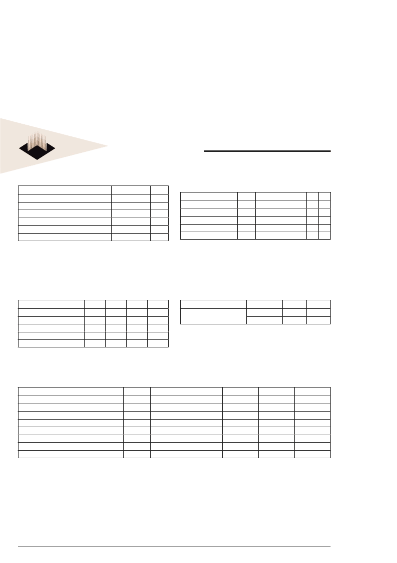
ABSOLUTE MAXIMUM RATINGS
Parameter
Operating Temperature
Supply Voltage Range (V
CC
)
Signal Voltage Range
Storage Temperature Range
Lead Temperature (soldering, 10 seconds)
Endurance (write/erase cycles)
NOTES:
1. Stresses above the absolute maximum rating may cause permanent damage to the
device. Extended operation at the maximum levels may degrade performance and
affect reliability.
Unit
°C
V
V
°C
°C
cycles
-55 to +125
-0.5 to +4.0
-0.5 to Vcc +0.5
-65 to +150
+300
1,000,000 min.
RECOMMENDED OPERATING CONDITIONS
Parameter
Symbol
Supply Voltage
V
CC
Input High Voltage
Input Low Voltage
Operating Temp. (Mil.)
Operating Temp. (Ind.)
Min
3.0
Max
3.6
Unit
V
V
V
°C
°C
V
IH
V
IL
T
A
T
A
0.7 x V
CC
V
CC
+ 0.3
-0.5
-55
-40
+0.8
+125
+85
CAPACITANCE
T
A
= +25°C
Symbol
C
OE
C
WE
C
CS
C
I/O
C
AD
Parameter
OE# capacitance
WE#1-4 capacitance
CS1-4 capacitance
Data I/O capacitance
Address input capacitance
This parameter is guaranteed by design but not tested.
Conditions
V
IN
= 0 V, f = 1.0 MHz
V
IN
= 0 V, f = 1.0 MHz
V
IN
= 0 V, f = 1.0 MHz
V
I/O
= 0 V, f = 1.0 MHz
V
IN
= 0 V, f = 1.0 MHz
Max Unit
50
20
20
20
50
pF
pF
pF
pF
pF
DC CHARACTERISTICS – CMOS COMPATIBLE
V
CC
= 3.3V, V
SS
= 0V, -55°C ≤ T
A
≤ +125°C
Symbol
I
LI
V
CC
= 3.6, V
IN
= GND or V
CC
I
LOx32
V
CC
= 3.6, V
IN
= GND or V
CC
I
CC1
CS# = V
IL
, OE# = V
IH
, f = 5MHz
I
CC2
CS# = V
IL
, OE# = V
IH
I
CC3
V
CC
= 3.6, CS = V
IH
, f = 5MHz
V
OL
I
OL
= 5.8 mA, V
CC
= 3.0
V
OH1
I
OH
= -2.0 mA, V
CC
= 3.0
V
LKO
Parameter
Input Leakage Current
Output Leakage Current
V
CC
Active Current for Read (1)
V
CC
Active Current for Program or Erase (2)
V
CC
Standby Current
Output Low Voltage
Output High Voltage
Low V
CC
Lock-Out Voltage (4)
NOTES:
1. The I
CC
current listed includes both the DC operating current and the frequency dependent component (at 5 MHz). The frequency component typically is less than 8 mA/MHz, with
OE# at V
IH
.
2. I
CC
active while Embedded Algorithm (program or erase) is in progress.
3. DC test conditions: V
IL
= 0.3V, V
IH
= V
CC
- 0.3V
4. Guaranteed by design, but not tested.
Conditions
Min
Max
10
10
120
140
200
0.45
Unit
μA
μA
mA
mA
μA
V
V
V
0.85
X
V
CC
2.3
2.5
DATA RETENTION
Test Conditions
Parameter
Minimum Pattern Data
Retention Time
Min
10
20
Unit
Years
Years
150°C
125°C
相關(guān)PDF資料 |
PDF描述 |
|---|---|
| WF1M32B-150HM3 | 1Mx32 3.3V Flash Module |
| WF1M32B-150HM3A | 1Mx32 3.3V Flash Module |
| WF1M32B-XXX3 | 1Mx32 3.3V Flash Module |
| WF1 | ASSEMBLY JIG PCB ALUMINIUM |
| WF2 | ASSEMBLY JIG PCB ALUMINIUM |
相關(guān)代理商/技術(shù)參數(shù) |
參數(shù)描述 |
|---|---|
| WF1M32B-150HM3 | 制造商:Microsemi Corporation 功能描述:1M X 32 FLASH MODULE, 3.3V, 150NS, BOOT BLOCK, 66 PGA 1.185" - Bulk |
| WF1M32B-150HM3A | 制造商:WEDC 制造商全稱(chēng):White Electronic Designs Corporation 功能描述:1Mx32 3.3V Flash Module |
| WF1M32BP-100G2TI5A | 制造商:未知廠家 制造商全稱(chēng):未知廠家 功能描述:x32 Flash EEPROM Module |
| WF1M32BP-100G2TM5A | 制造商:未知廠家 制造商全稱(chēng):未知廠家 功能描述:x32 Flash EEPROM Module |
| WF1M32BP-120G2TI5A | 制造商:未知廠家 制造商全稱(chēng):未知廠家 功能描述:x32 Flash EEPROM Module |
發(fā)布緊急采購(gòu),3分鐘左右您將得到回復(fù)。