- 您現(xiàn)在的位置:買賣IC網(wǎng) > PDF目錄371244 > X28LV010T-90 128Kx8 EEPROM PDF資料下載
參數(shù)資料
| 型號(hào): | X28LV010T-90 |
| 元件分類: | EEPROM |
| 英文描述: | 128Kx8 EEPROM |
| 中文描述: | 128Kx8 EEPROM |
| 文件頁數(shù): | 8/18頁 |
| 文件大小: | 141K |
| 代理商: | X28LV010T-90 |

X28LV010
Characteristics subject to change without notice.
8 of 18
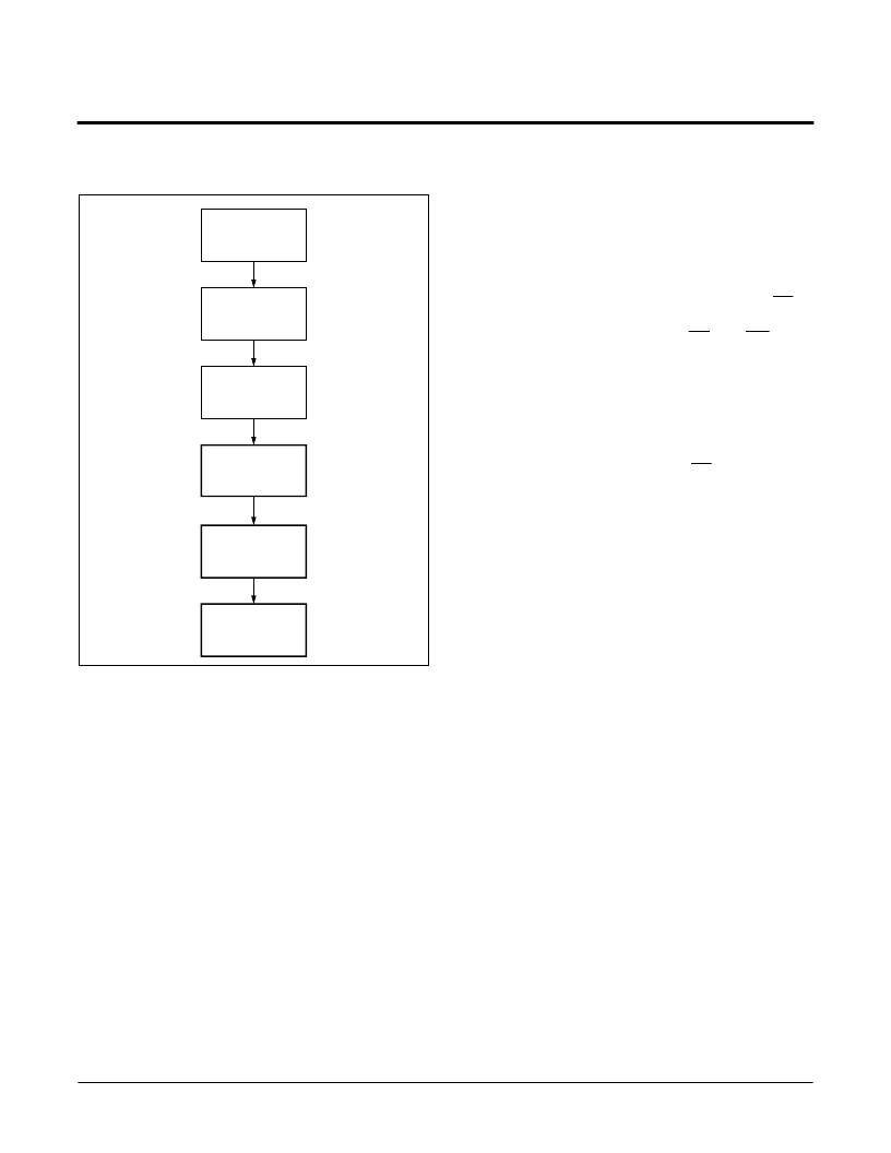
Figure 9. Software Sequence to Deactivate
Software Data Protection
In the event the user wants to deactivate the software
data protection feature for testing or reprogramming in
an E
2
PROM programmer, the following six step algo-
rithm will reset the internal protection circuit. After t
WC
,
the X28LV010 will be in standard operating mode.
Note:
Once initiated, the sequence of write operations
should not be interrupted.
SYSTEM CONSIDERATIONS
Because the X28LV010 is frequently used in large
memory arrays it is provided with a two line control
architecture for both read and write operations. Proper
usage can provide the lowest possible power dissipa-
tion and eliminate the possibility of contention where
multiple I/O pins share the same bus.
To gain the most benefit it is recommended that CE be
decoded from the address bus and be used as the pri-
mary device selection input. Both OE and WE would
then be common among all devices in the array. For a
read operation this assures that all deselected devices
are in their standby mode and that only the selected
device(s) is outputting data on the bus.
Because the X28LV010 has two power modes,
standby and active, proper decoupling of the memory
array is of prime concern. Enabling CE will cause tran-
sient current spikes. The magnitude of these spikes is
dependent on the output capacitive loading of the I/Os.
Therefore, the larger the array sharing a common bus,
the larger the transient spikes. The voltage peaks
associated with the current transients can be sup-
pressed by the proper selection and placement of
decoupling capacitors. As a minimum, it is recom-
mended that a 0.1μF high frequency ceramic capacitor
be used between V
CC
and V
SS
at each device.
Depending on the size of the array, the value of the
capacitor may have to be larger.
In addition, it is recommended that a 4.7μF electrolytic
bulk capacitor be placed between V
CC
and V
SS
for
each eight devices employed in the array. This bulk
capacitor is employed to overcome the voltage drop
caused by the inductive effects of the PC board traces.
2AAA
Write Data 55
to Address
2AAA
Write Data 80
to Address
5555
5555
Write Data 20
to Address
5555
Write Data AA
to Address
5555
Write Data AA
to Address
Write Data 55
to Address
相關(guān)PDF資料 |
PDF描述 |
|---|---|
| X28LV010TI-12 | HD,CRYPTOMEM,256KBIT,WAFER(EMBEDDED CRYPTO PROD) |
| X28LV010TI-15 | 128Kx8 EEPROM |
| X28LV010TI-70 | 128Kx8 EEPROM |
| X28LV010TI-90 | 128Kx8 EEPROM |
| X28LV010JI-15 | 128Kx8 EEPROM |
相關(guān)代理商/技術(shù)參數(shù) |
參數(shù)描述 |
|---|---|
| X28LV010TI-12 | 制造商:未知廠家 制造商全稱:未知廠家 功能描述:x8 EEPROM |
| X28LV010TI-15 | 制造商:未知廠家 制造商全稱:未知廠家 功能描述:x8 EEPROM |
| X28LV010TI-70 | 制造商:未知廠家 制造商全稱:未知廠家 功能描述:x8 EEPROM |
| X28LV010TI-90 | 制造商:未知廠家 制造商全稱:未知廠家 功能描述:x8 EEPROM |
| X28RT | 制造商:BURNDY 功能描述:BURNDY PRODUCTS TOOLING |
發(fā)布緊急采購,3分鐘左右您將得到回復(fù)。