- 您現(xiàn)在的位置:買賣IC網(wǎng) > PDF目錄371269 > X68C75L Port Expander and E2 Memory PDF資料下載
參數(shù)資料
| 型號: | X68C75L |
| 英文描述: | Port Expander and E2 Memory |
| 中文描述: | 端口擴(kuò)展和E2內(nèi)存 |
| 文件頁數(shù): | 8/26頁 |
| 文件大小: | 123K |
| 代理商: | X68C75L |
第1頁第2頁第3頁第4頁第5頁第6頁第7頁當(dāng)前第8頁第9頁第10頁第11頁第12頁第13頁第14頁第15頁第16頁第17頁第18頁第19頁第20頁第21頁第22頁第23頁第24頁第25頁第26頁

8
X68C75 SLIC
E
2
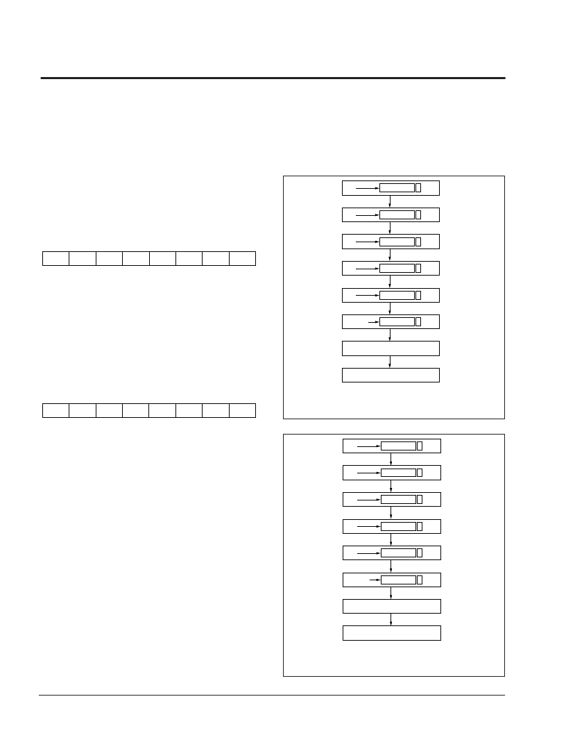
Figure 8. Setting the SFR Map Register
Figure 9. Setting Program Memory Map Register
Programmable Address Decoding
The X68C75 features an internal programmable ad-
dress decoder which allows the nonvolatile memory
array and the internal registers to be mapped in various
locations of the 64K-byte memory map. The register set
is mappable into a 1K-byte block, while the nonvolatile
memory array is mappable into an 8K-byte block. The
mapping is controlled by two nonvolatile configuration
registers, the SFR Map Register and the E
2
Memory
Map Register. Their bits are mapped as follows:
SFR Map Register (SFRM) Default = 81
1
0
A15
A14
A13
A12
A11
A10
7
6
2899 ILL F08
5
4
3
2
1
0
A15-A10
A15-A10 are upper address bits for the 1K-byte page
where the SFR memory is mapped.
BITS 7:6
Setting these two bits to any combination other than “10”
will interfere with device proper operation.
E
2
Memory Map Register (EEM) Default = 07
0
0
LAM
0
RST
A15
A14
A13
7
6
2899 ILL F09
5
4
3
2
1
0
A15-A13
Modifying these three bits changes the location of the
program memory within the address map.The A15-A13
correspond to the upper three address bits of the 8K-
byte page where program memory will be mapped.
RST
The RST bit controls the polarity of the RESET input pin.
“0” = RESET is Active LOW
“1” = RESET is Active HIGH
LAM
Port B can be configured as either a general purpose
I/O port (normal I/O mode), or latched address mode
(LAM). The LAM option programs port B to output the
demultiplexed low order byte of the address latched into
the X68C75 by AS. The LAM bit selects between these
two modes.
“0” = Port B is an I/O Port
“1” = Port B outputs low address byte (A7-A0)
AA
b2
P 555
b1 b0
55
b2
AAA
AAA
b1 b0
A0
b2
P 555
b1 b0
AA
b2
P 555
b1 b0
D0
Delay of t
WC
Exit Routine
b2
P
2899 ILL F10.1
b1 b0
XXX
Desired
Value
b2
P
b1 b0
BX = Don’t Care
P = Address bit (A12) of the
memory plane not being read.
P
AA
b2
P 555
b1 b0
55
b2
AAA
AAA
b1 b0
A0
b2
P 555
b1 b0
AA
b2
P 555
b1 b0
E0
b2
P
2899 ILL F11.1
b1 b0
XXX
Desired
Value
b2
P
b1 b0
BX = Don’t Care
P = Address bit (A12) of the
memory plane not being read.
P
Delay of t
WC
Exit Routine
Setting the Mapping Registers
The mapping registers are written using a modified
version of the Software Data Protection sequence. All
timings must adhere to the normal Software Data
Protection sequence.
相關(guān)PDF資料 |
PDF描述 |
|---|---|
| X68C75LI | Port Expander and E2 Memory |
| X68C75LM | Port Expander and E2 Memory |
| X68C75P | Port Expander and E2 Memory |
| X68C75PI | Port Expander and E2 Memory |
| X68C75PM | Port Expander and E2 Memory |
相關(guān)代理商/技術(shù)參數(shù) |
參數(shù)描述 |
|---|---|
| X68C75LI | 制造商:XICOR 制造商全稱:Xicor Inc. 功能描述:Port Expander and E2 Memory |
| X68C75LM | 制造商:XICOR 制造商全稱:Xicor Inc. 功能描述:Port Expander and E2 Memory |
| X68C75P | 制造商:XICOR 制造商全稱:Xicor Inc. 功能描述:Port Expander and E2 Memory |
| X68C75PI | 制造商:XICOR 制造商全稱:Xicor Inc. 功能描述:Port Expander and E2 Memory |
| X68C75PM | 制造商:XICOR 制造商全稱:Xicor Inc. 功能描述:Port Expander and E2 Memory |
發(fā)布緊急采購,3分鐘左右您將得到回復(fù)。