- 您現(xiàn)在的位置:買賣IC網(wǎng) > PDF目錄371269 > X68C75LM Port Expander and E2 Memory PDF資料下載
參數(shù)資料
| 型號: | X68C75LM |
| 英文描述: | Port Expander and E2 Memory |
| 中文描述: | 端口擴(kuò)展和E2內(nèi)存 |
| 文件頁數(shù): | 5/26頁 |
| 文件大?。?/td> | 123K |
| 代理商: | X68C75LM |
第1頁第2頁第3頁第4頁當(dāng)前第5頁第6頁第7頁第8頁第9頁第10頁第11頁第12頁第13頁第14頁第15頁第16頁第17頁第18頁第19頁第20頁第21頁第22頁第23頁第24頁第25頁第26頁

5
X68C75 SLIC
E
2
Software Data Protection
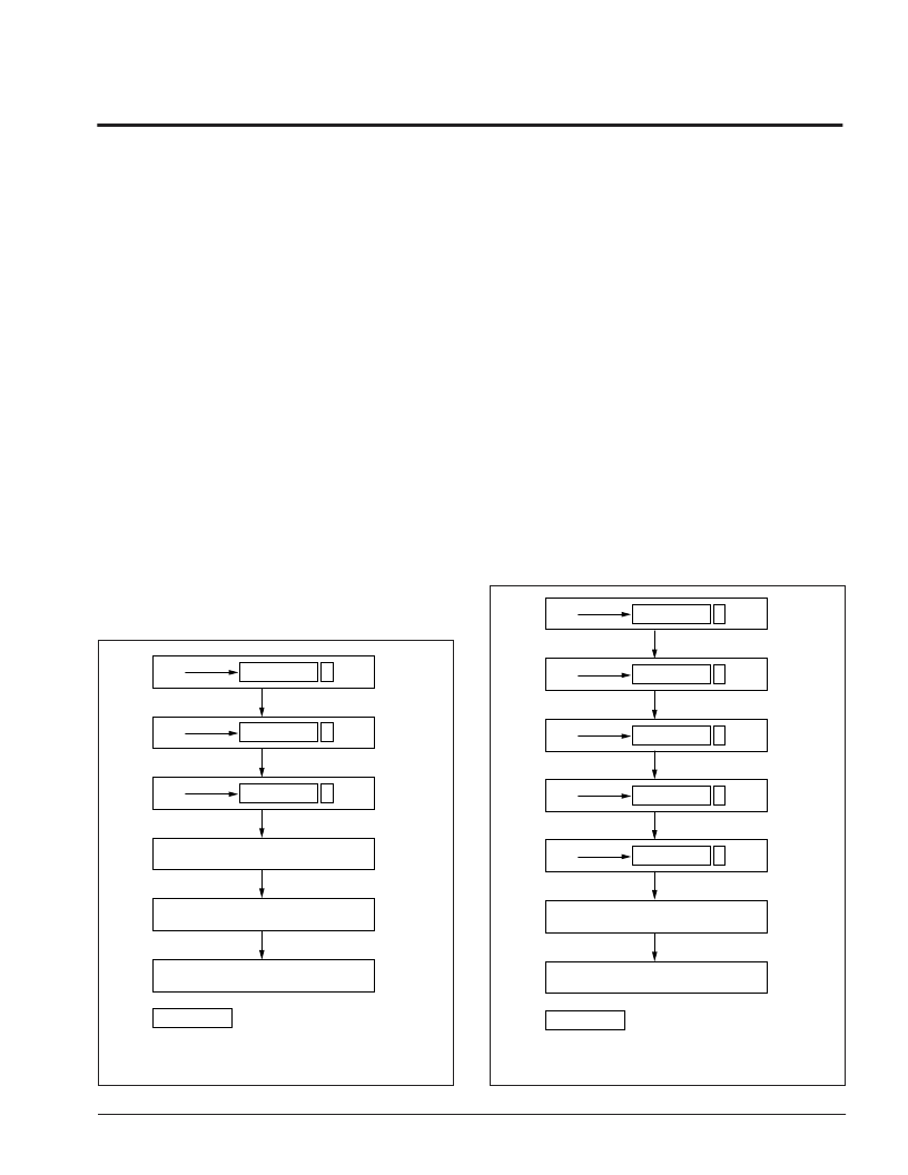
Software Data Protection (SDP) can be employed to
protect the entire array against inadvertent writes during
power-up/power-down operations. The X68C75 is
shipped from the factory with SDP enabled. With SDP
enabled, inadvertent attempts to write to the X68C75 will
be blocked.
The system can still write data, but only when the write
operation (page or byte) is preceded by the three-byte
command sequence. All write operations, both the com-
mand sequence and any data write operations must
conform to the page write timing requirements.
The SDP mode is also enabled anytime one of the
nonvolatile configuration registers are modified. These
include writing to EE map, SFR map, and BPR.
Block Lock Protect Write Lockout
The X68C75 provides a second level of data security
referred to as Block Lock Protect write lockout (or Block
Protection). This is accessed through an extension of
the SDP command sequence. Block Protect allows the
user to lockout writes to 1K x 8 blocks of memory. Unlike
SDP which prevents inadvertent writes, but still allows
easy system access to writing the memory, Block Pro-
tect will lockout all attempts unless it is specifically
disabled by issuing the deactivation sequence. This
feature can be used to set a higher level of protection in
a system where a portion of the memory is used to store
the system kernel and protect it from the application
programs residing in the other blocks.
Setting write lockout is accomplished by writing a five-
byte command sequence opening access to the Block
Protect Register (BPR). After the fifth byte is written, the
user writes to the BPR, selecting which blocks to protect
or unprotect. All write operations, both the command
sequence and writing the data to the BPR, must conform
to the page write timing requirements. It should be noted
that accessing the BPR automatically sets the upper
level SDP. If for some reason the user does not want
SDP enabled, they may reset it using the normal reset
command sequence. This will not affect the state of the
BPR and any 1K x 8 blocks that were set to the write
lockout state will remain in the write lockout state.
AA
b2
P 555
b1 b0
55
b2
AAA
b1 b0
A0
b2
P 555
b1 b0
2899 ILL F05C
Reference the A15–A13
setting in EEM register
Delay of t
WC
Exit Routine
P = Address bit (A12) of the
memory plane not being read.
b2 b1 b0
P
AA
b2
P 555
b1 b0
80
b2
P AAA
b1 b0
Figure 3. Sequence to Deactivate
Software Data Protection
AA
b2
P 555
b1 b0
55
b2
AAA
b1 b0
A0
b2
P 555
b1 b0
2899 ILL F05B
Perform Byte or Page
Write Operations
Reference the A15–A13
setting in EEM register
Delay of t
WC
Exit Routine
P = Address bit (A12) of the
updated memory plane.
b2 b1 b0
P
Figure 2. Writing with SDP Enabled
相關(guān)PDF資料 |
PDF描述 |
|---|---|
| X68C75P | Port Expander and E2 Memory |
| X68C75PI | Port Expander and E2 Memory |
| X68C75PM | Port Expander and E2 Memory |
| X76041PI | Serial EEPROM |
| X76041PI-3 | Serial EEPROM |
相關(guān)代理商/技術(shù)參數(shù) |
參數(shù)描述 |
|---|---|
| X68C75P | 制造商:XICOR 制造商全稱:Xicor Inc. 功能描述:Port Expander and E2 Memory |
| X68C75PI | 制造商:XICOR 制造商全稱:Xicor Inc. 功能描述:Port Expander and E2 Memory |
| X68C75PM | 制造商:XICOR 制造商全稱:Xicor Inc. 功能描述:Port Expander and E2 Memory |
| X68EM05JB4 | 制造商:Motorola Inc 功能描述: |
| X68EM05PV8 | 制造商:Motorola Inc 功能描述: |
發(fā)布緊急采購,3分鐘左右您將得到回復(fù)。