- 您現(xiàn)在的位置:買賣IC網(wǎng) > PDF目錄371269 > X68C75PI Port Expander and E2 Memory PDF資料下載
參數(shù)資料
| 型號: | X68C75PI |
| 英文描述: | Port Expander and E2 Memory |
| 中文描述: | 端口擴展和E2內(nèi)存 |
| 文件頁數(shù): | 10/26頁 |
| 文件大小: | 123K |
| 代理商: | X68C75PI |

10
X68C75 SLIC
E
2
Configuration Register (CR)
The Configuration Register is a volatile register used to
configure the operation of the I/O ports. The configura-
tion register allows the microcontroller to designate
whether each of the two ports is an input or output, what
type of output drive is to be used, and specifies the
polarity of the two strobe lines, STRA and STRB. The bit
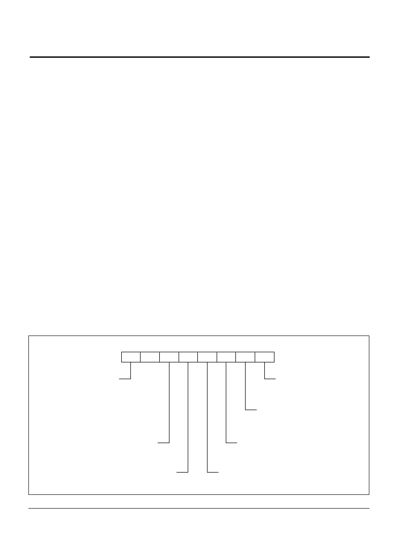
map of configuration register is shown below.
The IRST bit in the configuration register controls the
method used to clear the port interrupt request flags
(INTA, INTB). The interrupts are reset by either reading
the interrupt source or writing to the interrupt status
register. The interrupt must be disabled prior to chang-
ing strobe polarity bits (STPA, STPB), or port direction
bits (DIRA, DIRB) in CR. Otherwise, any attempt to
modify the status of these bits may cause an interrupt to
occur.
Port Data Registers (PDR)
The PDRA/PDRB are byte-wide latches which hold port
data. When a port is configured as an output, the outputs
of its PDR latch are connected to the port pins. Writing
to PDR generates a pulse on the port strobe pin and
latches the data. If a port is configured as an input, the
inputs of its PDR latch are connected to the port pins.
External data is latched into PDR on the positive edge of
its clock. The port strobe input and strobe polarity bit
(STPA, STPB) are XORed to generate the PDR input
clock.
Port Pin Registers (PPR)
The read-only Port Pin Registers are used for reading
the current status of the external I/O port pins. Accessing
the PPR causes the values on the port pins to be placed
on the data bus.
The port direction control bits in configuration register
set the direction for the entire port and no control
mechanism is provided to program the direction of
individual pins. However, the ports have a flexible archi-
tecture which allows operating I/O ports in bidirectional
mode using the PPR read feature.
A port can be operated in input/output mode by config-
uring it as an open-drain output port. The port wire-OR
bit (AWO, or BW) and its port data direction bit (DIRA,
or DIRB) in CR, should be set to “1”. The PDR bits which
correspond to the port pins assigned as inputs should be
programmed to “1”. For monitoring the status of the input
pins, the PPR can be read. In this application the port
strobe pin and the PDR latch are in output mode. In
open-drain mode, there are weak internal pull-ups on
the port pins, however external pull-ups must be used for
proper switching of the I/O lines.
Static RAM Block
There are 16 bytes of volatile static RAM registers
mapped to the SFR region. They reside in the 200H-
20FH area offset from the SFR base address. Accessing
these registers has to be done through external RAM
operations for both writes and reads.
Figure 11. Configuration Register
IRST
2899 ILL F13.1
1
AWO BWO DIRA DIRB STPA STPB
7
6
5
4
3
2
1
0
Interrupt Request Reset Mode
This bit controls the clearing of the
interrupt request flag.
“0” = Reading the interrupt source
“1” = Writing to the request register
Port A – Outputs
“0” = CMOS
“1” = Open-Drain
Port B – Outputs
“0” = CMOS
“1” = Open-Drain
Port A – Direction Flag
“0” = Input mode
“1” = Output mode
Port B – Direction Flag
“0” = Input mode
“1” = Output mode
Strobe B – Strobe Pin Polarity
“0” = Active LOW
“1” = Active HIGH
Strobe A – Strobe Pin Polarity
“0” = Active LOW
“1” = Active HIGH
相關(guān)PDF資料 |
PDF描述 |
|---|---|
| X68C75PM | Port Expander and E2 Memory |
| X76041PI | Serial EEPROM |
| X76041PI-3 | Serial EEPROM |
| X76041S | Serial EEPROM |
| X76041S-3 | Serial EEPROM |
相關(guān)代理商/技術(shù)參數(shù) |
參數(shù)描述 |
|---|---|
| X68C75PM | 制造商:XICOR 制造商全稱:Xicor Inc. 功能描述:Port Expander and E2 Memory |
| X68EM05JB4 | 制造商:Motorola Inc 功能描述: |
| X68EM05PV8 | 制造商:Motorola Inc 功能描述: |
| X68EML05P6A | 制造商:Freescale Semiconductor 功能描述:Tools Emulator For Use With:6 |
| X68HC705H12PGMR | 制造商:Motorola 功能描述:MOTOROLA S7D6A |
發(fā)布緊急采購,3分鐘左右您將得到回復。