- 您現(xiàn)在的位置:買賣IC網(wǎng) > PDF目錄371269 > X68C75PI Port Expander and E2 Memory PDF資料下載
參數(shù)資料
| 型號(hào): | X68C75PI |
| 英文描述: | Port Expander and E2 Memory |
| 中文描述: | 端口擴(kuò)展和E2內(nèi)存 |
| 文件頁數(shù): | 11/26頁 |
| 文件大?。?/td> | 123K |
| 代理商: | X68C75PI |
第1頁第2頁第3頁第4頁第5頁第6頁第7頁第8頁第9頁第10頁當(dāng)前第11頁第12頁第13頁第14頁第15頁第16頁第17頁第18頁第19頁第20頁第21頁第22頁第23頁第24頁第25頁第26頁

11
X68C75 SLIC
E
2
PRINCIPLES OF OPERATION
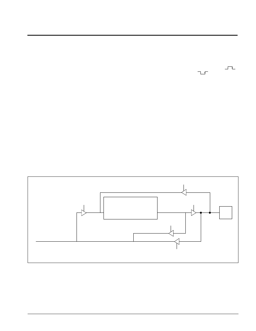
I/O Ports Operation
The expansion ports are accessible to the software
using their assigned memory mapped addresses. Each
port occupies two addresses in the SFR plane, the Port
Data Register and Port Pin Register. These registers
and their location in the 1K-byte register memory space
is shown on page 7.
The ports can be configured as either inputs or outputs,
the DIRA and DIRB bits in the configuration register are
used to select between the modes. The input signal on
the strobe pin, when the corresponding port is config-
ured as an input, is fed to the clock input of the port latch.
These are transparent latches and the trailing edge of
the strobe pulse is used to latch the data present on the
input pins. The strobe signal polarity is configurable
using the STPA and STPB bits in the configuration
register.
Writing to the port data register of an output port will
generate a pulse of fixed duration on its strobe pin. The
data also simultaneously arrives at the port output pins.
The latched data stays there until new data is written to
the port data register. The strobe pulse shape is con-
trolled by the state of the STPA and STPB bits in
configuration register. A “1” forces the valid transition on
the corresponding strobe pin as active HIGH (
and a “0” sets it to active LOW (
),
) .
When an external strobe signal is applied to an input
port, the latching of input data is followed by the setting
of the interrupt flags. The INTA and INTB interrupt flags
are used by ports A and B respectively, and are set along
with the INT interrupt flag at the end of strobe pulse input.
External interrupt (
IRQ
) is generated if the interrupt
enable flags (ENA, and ENB) are set by the software.
The former enables the port A interrupt and the latter the
port B interrupt.
The port output drivers can be either CMOS or open-
drain. The wire-OR bits (AWO, BWO) in the configura-
tion register are used to make the selection. When the
bits are “0” the CMOS drivers are enabled . Setting these
bits will enable the open-drain output drivers. Small pull-
up resistors should be used on the pins of open-drain
outputs.
Figure 12. Block Diagram of the I/O Ports
INTERNAL DATA BUS
I/O
PIN
PORT
OUTPUT
OUTPUT
INPUT
LATCH FOR
I/O PIN
PORT WRITE
(PORT OUTPUT)
STROBE (PORT INPUT)
2899 ILL F14.1
PORT READ
(PORT INPUT)
PIN READ
(PORT IN OR OUTPUT)
相關(guān)PDF資料 |
PDF描述 |
|---|---|
| X68C75PM | Port Expander and E2 Memory |
| X76041PI | Serial EEPROM |
| X76041PI-3 | Serial EEPROM |
| X76041S | Serial EEPROM |
| X76041S-3 | Serial EEPROM |
相關(guān)代理商/技術(shù)參數(shù) |
參數(shù)描述 |
|---|---|
| X68C75PM | 制造商:XICOR 制造商全稱:Xicor Inc. 功能描述:Port Expander and E2 Memory |
| X68EM05JB4 | 制造商:Motorola Inc 功能描述: |
| X68EM05PV8 | 制造商:Motorola Inc 功能描述: |
| X68EML05P6A | 制造商:Freescale Semiconductor 功能描述:Tools Emulator For Use With:6 |
| X68HC705H12PGMR | 制造商:Motorola 功能描述:MOTOROLA S7D6A |
發(fā)布緊急采購(gòu),3分鐘左右您將得到回復(fù)。