- 您現(xiàn)在的位置:買賣IC網(wǎng) > PDF目錄371269 > X76F100P-3.0 1K 128 x 8 Bit PDF資料下載
參數(shù)資料
| 型號(hào): | X76F100P-3.0 |
| 英文描述: | 1K 128 x 8 Bit |
| 中文描述: | 每1000 128 × 8位 |
| 文件頁數(shù): | 8/17頁 |
| 文件大小: | 275K |
| 代理商: | X76F100P-3.0 |

X76F100
Characteristics subject to change without notice.
8 of 16
REV 1.0 6/22/00
www.xicor.com
ABSOLUTE MAXIMUM RATINGS
Temperature under bias ....................–65°C to +135°C
Storage temperature ........................–65°C to +150°C
Voltage on any pin with
respect to V
SS
.........................................–1V to +7V
D.C. output current ...............................................5mA
Lead temperature (soldering, 10 seconds).........300°C
COMMENT
Stresses above those listed under “Absolute Maximum
Ratings” may cause permanent damage to the device.
This is a stress rating only; functional operation of the
device (at these or any other conditions above those
listed in the operational sections of this specification) is
not implied. Exposure to absolute maximum rating con-
ditions for extended periods may affect device reliability.
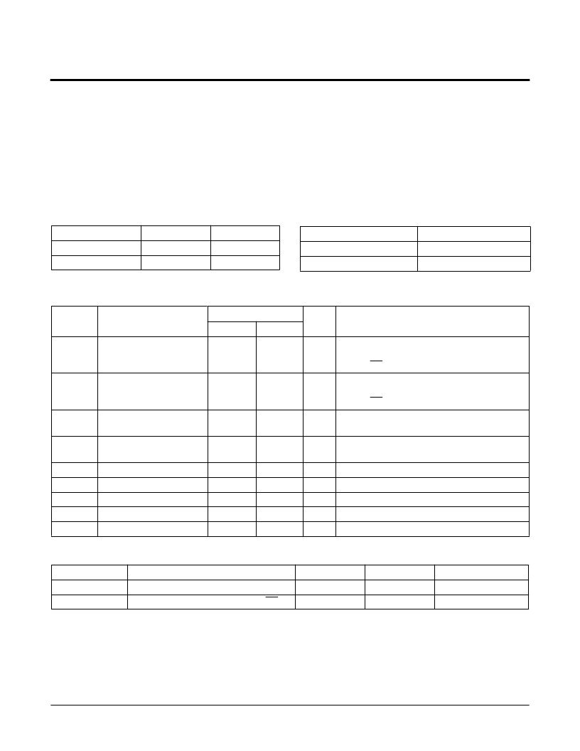
RECOMMENDED OPERATING CONDITIONS
Temperature
Commercial
Industrial
Min.
0°C
–40°C
Max.
+70°C
+85°C
Supply Voltage
X76F100
X76F100-3
Limits
4.5V to 5.5V
3.0V to 5.5V
D.C. OPERATING CHARACTERISTICS
(Over the recommended operating conditions unless otherwise specified.)
CAPACITANCE
T
A
= +25°C, f = 1MHz, V
CC
= 5V
Notes:
(1) Must perform a stop command after a read command prior to measurement.
(2) V
IL
min. and V
IH
max. are for reference only and are not tested.
(3) This parameter is periodically sampled and not 100% tested.
Symbol
I
CC1
Parameter
Supply Current
(Read)
Limits
Unit
mA
Test Conditions
x 0.1/V
CC
x 0.9 Levels @ 400 kHz,
SDA = Open
RST = CS = V
SS
f
SCL
= V
CC
x 0.1/V
CC
x 0.9 Levels @ 400 kHz,
SDA = Open
RST = CS = V
SS
V
IL
= V
CC
x 0.1, V
IH
= V
f
SCL
= 400 kHz, f
SDA
= 400 kHz
V
SDA
= V
SCC
= V
CC
Other = GND or V
CC
–0.3V
V
IN
= V
SS
to V
CC
V
OUT
= V
SS
to V
CC
Min.
Max.
1
V
CC
f
SCL
= V
CC
I
CC2
(3)
V
(Write)
CC
Supply Current
3
mA
I
SB1
(1)
V
(Standby)
CC
Supply Current
1
μA
CC
x 0.9
I
SB2
(1)
V
(Standby)
CC
Supply Current
1
μA
I
LI
I
LO
V
IL
(2)
V
IH
(2)
V
OL
Input Leakage Current
Output Leakage Current
Input LOW Voltage
Input HIGH Voltage
Output LOW Voltage
10
10
μA
μA
V
V
V
–0.5
V
CC
x 0.3
V
CC
+ 0.5
0.4
V
CC
x 0.7
I
OL
= 3mA
Symbol
C
OUT
(3)
C
IN
(3)
Test
Max.
8
6
Unit
pF
pF
Conditions
V
I/O
= 0V
V
IN
= 0V
Output Capacitance (SDA)
Input Capacitance (RST, SCL, CS)
相關(guān)PDF資料 |
PDF描述 |
|---|---|
| X76F100PI | 1K 128 x 8 Bit |
| X76F100PI-3.0 | 1K 128 x 8 Bit |
| X76F100S8 | 1K 128 x 8 Bit |
| X76F100S8-3.0 | 1K 128 x 8 Bit |
| X76F100S8I | CLAMP |
相關(guān)代理商/技術(shù)參數(shù) |
參數(shù)描述 |
|---|---|
| X76F100PI | 制造商:XICOR 制造商全稱:Xicor Inc. 功能描述:1K 128 x 8 Bit |
| X76F100PI-3.0 | 制造商:XICOR 制造商全稱:Xicor Inc. 功能描述:1K 128 x 8 Bit |
| X76F100S8 | 制造商:XICOR 制造商全稱:Xicor Inc. 功能描述:1K 128 x 8 Bit |
| X76F100S8-3.0 | 制造商:XICOR 制造商全稱:Xicor Inc. 功能描述:1K 128 x 8 Bit |
| X76F100S8I | 制造商:XICOR 制造商全稱:Xicor Inc. 功能描述:1K 128 x 8 Bit |
發(fā)布緊急采購,3分鐘左右您將得到回復(fù)。