- 您現(xiàn)在的位置:買賣IC網(wǎng) > PDF目錄376449 > X9525B20I (INTERSIL CORP) Fiber Channel/Gigabit Etherner Laser Diode Control for Fiber Optic Modules PDF資料下載
參數(shù)資料
| 型號: | X9525B20I |
| 廠商: | INTERSIL CORP |
| 元件分類: | 數(shù)字電位計 |
| 英文描述: | Fiber Channel/Gigabit Etherner Laser Diode Control for Fiber Optic Modules |
| 中文描述: | DUAL 50K DIGITAL POTENTIOMETER, 2-WIRE SERIAL CONTROL INTERFACE, 256 POSITIONS, BGA20 |
| 封裝: | CSP-20 |
| 文件頁數(shù): | 8/26頁 |
| 文件大?。?/td> | 578K |
| 代理商: | X9525B20I |
第1頁第2頁第3頁第4頁第5頁第6頁第7頁當(dāng)前第8頁第9頁第10頁第11頁第12頁第13頁第14頁第15頁第16頁第17頁第18頁第19頁第20頁第21頁第22頁第23頁第24頁第25頁第26頁

8
FN8210.0
March 10, 2005
It should be noted that all writes to any DCP of the X9525
are random in nature. Therefore, the Data Byte of con-
secutive write operations to any DCP can differ by an
arbitrary number of bits. Also, setting the bits (P1 = 0,
P0 = 0) or (P1 = 1, P0 = 1) are reserved sequences, and
will result in no ACKNOWLEDGE after sending an
Instruction Byte on SDA.
The factory default setting of all “wiper position” settings
is with 00h stored in the NVM of the DCPs. This corre-
sponds to having the “wiper teminal”
R
WX
(x = 1,2) at the
“l(fā)owest” tap position, therefore, the resistance between
R
WX
and
R
LX
is a minimum (essentially only the Wiper
Resistance,
R
W
).
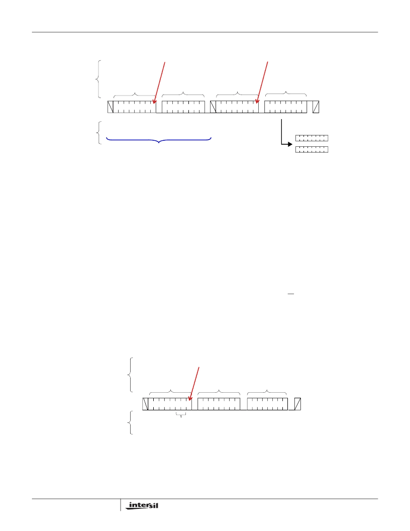
DCP Read Operation
A read of DCPx (x = 1,2) can be performed using the
three byte random read command sequence shown in
Figure 10.
The master issues the START condition and the Slave
Address Byte 1010A
0
110 which specifies that a
“dummy” write” is to be conducted. This “dummy” write
operation sets which DCP is to be read (in the preceding
Read operation). An ACKNOWLEDGE is returned by the
X9525 after the Slave Address if received correctly. Next,
an Instruction Byte is issued on SDA. Bits P1 - P0 of the
Instruction Byte determine which DCP “wiper position” is
to be read. In this case, the state of the WT bit is “don’t
care”. If the Instruction Byte format is valid, then another
ACKNOWLEDGE is returned by the X9525.
Following this ACKNOWLEDGE, the master immediately
issues another START condition and a valid Slave
address byte with the R/W bit set to 1. Then the X9525
issues an ACKNOWLEDGE followed by Data Byte, and
finally, the master issues a STOP condition. The Data
Byte read in this operation, corresponds to the “wiper
position” (value of the WCR) of the DCP pointed to by
bits P1 and P0.
Slave
Address
Instruction
Byte
A
C
K
A
C
K
S
t
a
r
t
S
t
o
p
Slave
Address
Data Byte
A
C
K
S
t
a
r
t
SDA Bus
Signals from
the Slave
Signals from
the Master
Figure 10. DCP Read Sequence
“Dummy” write
READ Operation
101
11
0
0
00 00
W
T
P
1
P
0
101
11
1
0
WRITE Operation
-
MSB
LSB
DCPx
x = 1
x = 2
“-” = DON’T CARE
A
0
A
0
S
t
a
r
t
S
t
o
p
Slave
Address
Address
Byte
Data
Byte
A
C
K
A
C
K
A
C
K
SDA Bus
Signals from
the Slave
Signals from
the Master
Figure 11. EEPROM Byte Write Sequence
Internal
Device
Address
1 0 1 0
00
0
WRITE Operation
A
0
X9525
相關(guān)PDF資料 |
PDF描述 |
|---|---|
| X9525 | Fiber Channel/Gigabit Etherner Laser Diode Control for Fiber Optic Modules |
| X9525V20I | Fiber Channel/Gigabit Etherner Laser Diode Control for Fiber Optic Modules |
| X9530 | Temperature Compensated Laser Diode Controller(帶溫度補償?shù)募す舛O管控制器) |
| X95840 | Quad Digital Controlled Potentiometers |
| X95840WV20I-2.7 | Quad Digital Controlled Potentiometers |
相關(guān)代理商/技術(shù)參數(shù) |
參數(shù)描述 |
|---|---|
| X9525BZ WAF | 制造商:Intersil Corporation 功能描述: |
| X9525V20I | 功能描述:IC DCP DUAL EEPROM MEM 20-TSSOP RoHS:否 類別:集成電路 (IC) >> PMIC - 激光驅(qū)動器 系列:- 產(chǎn)品培訓(xùn)模塊:Lead (SnPb) Finish for COTS Obsolescence Mitigation Program 標準包裝:60 系列:- 類型:激光二極管驅(qū)動器 數(shù)據(jù)速率:- 通道數(shù):4 電源電壓:3.3V 電流 - 電源:- 電流 - 調(diào)制:- 電流 - 偏置:- 工作溫度:0°C ~ 70°C 封裝/外殼:40-TQFN 裸露焊盤 供應(yīng)商設(shè)備封裝:40-TQFN EP 包裝:托盤 安裝類型:表面貼裝 |
| X9525V20IT1 | 功能描述:IC DCP DUAL EEPROM MEM 20-TSSOP RoHS:否 類別:集成電路 (IC) >> PMIC - 激光驅(qū)動器 系列:- 產(chǎn)品培訓(xùn)模塊:Lead (SnPb) Finish for COTS Obsolescence Mitigation Program 標準包裝:60 系列:- 類型:激光二極管驅(qū)動器 數(shù)據(jù)速率:- 通道數(shù):4 電源電壓:3.3V 電流 - 電源:- 電流 - 調(diào)制:- 電流 - 偏置:- 工作溫度:0°C ~ 70°C 封裝/外殼:40-TQFN 裸露焊盤 供應(yīng)商設(shè)備封裝:40-TQFN EP 包裝:托盤 安裝類型:表面貼裝 |
| X9525V20IZ | 制造商:INTERSIL 制造商全稱:Intersil Corporation 功能描述:Dual DCP, EEPROM Memory |
| X9530 | 制造商:INTERSIL 制造商全稱:Intersil Corporation 功能描述:Temperature Compensated Laser Diode Controller |
發(fā)布緊急采購,3分鐘左右您將得到回復(fù)。