- 您現(xiàn)在的位置:買賣IC網(wǎng) > PDF目錄376449 > X9530 (Intersil Corporation) Temperature Compensated Laser Diode Controller(帶溫度補(bǔ)償?shù)募す舛O管控制器) PDF資料下載
參數(shù)資料
| 型號: | X9530 |
| 廠商: | Intersil Corporation |
| 英文描述: | Temperature Compensated Laser Diode Controller(帶溫度補(bǔ)償?shù)募す舛O管控制器) |
| 中文描述: | 溫度補(bǔ)償激光二極管控制器(帶溫度補(bǔ)償?shù)募す舛O管控制器) |
| 文件頁數(shù): | 4/28頁 |
| 文件大小: | 372K |
| 代理商: | X9530 |
第1頁第2頁第3頁當(dāng)前第4頁第5頁第6頁第7頁第8頁第9頁第10頁第11頁第12頁第13頁第14頁第15頁第16頁第17頁第18頁第19頁第20頁第21頁第22頁第23頁第24頁第25頁第26頁第27頁第28頁

4
FN8211.1
November 11, 2005
PRINCIPLES OF OPERATION
CONTROL AND STATUS REGISTERS
The Control and Status Registers provide the user
with a mechanism for changing and reading the value
of various parameters of the X9530. The X9530
contains seven Control, one Status, and several
Reserved registers, each being one Byte wide (See
Figure 1). The Control registers 0 through 6 are
located at memory addresses 80h through 86h
respectively. The Status register is at memory address
87h, and the Reserved registers at memory address
88h through 8Fh.
All bits in Control register 6 always power-up to the
logic state “0”. All bits in Control registers 0 through 5
power-up to the logic state value kept in their
corresponding
nonvolatile
nonvolatile bits of a register retain their stored values
even when the X9530 is powered down, then powered
back up. The nonvolatile bits in Control 0 through
Control 5 registers are all preprogrammed to the logic
state “0” at the factory.
memory
cells.
The
Bits indicated as “Reserved” are ignored when read,
and must be written as “0”, if any Write operation is
performed to their registers.
A detailed description of the function of each of the
Control and Status register bits follows:
Control Register 0
This register is accessed by performing a Read or
Write operation to address 80h of memory.
BL1, BL0: B
LOCK
L
OCK
PROTECTION
BITS
(N
ON
-
VOLATILE
)
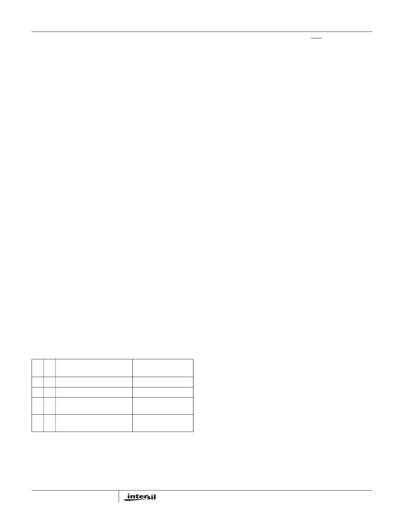
These two bits are used to inhibit any write operation
to certain addresses within the memory array. The
protected region of memory is determined by the
values of the two bits as shown in the table below:
If the user attempts to perform a write operation to a
protected region of memory, the operation is aborted
without changing any data in the array.
Notice that if the Write Protect (WP) input pin of the
X9530 is active (LOW), then any write operation to
the memory is inhibited, irrespective of the Block
Lock bit settings.
VRM: V
OLTAGE
R
EFERENCE
PIN
M
ODE
(N
ON
-
VOLATILE
)
The VRM bit configures the Voltage Reference pin
(VRef) as either an input or an output. When the VRM
bit is set to “0” (default), the voltage at pin VRef is an
output from the X9530’s internal voltage reference.
When the VRM bit is set to “1”, the voltage reference
for the VRef pin is external. See Figure 2.
ADCIN: A/D C
ONVERTER
I
NPUT
S
ELECT
(N
ON
-
VOLATILE
)
The ADCIN bit selects the input of the on-chip A/D
converter. When the ADCIN bit is set to “0” (default),
the output of the on-chip temperature sensor is the
input to the A/D converter. When the ADCIN bit is set
to “1”, the input to the A/D converter is the voltage at
the VSense pin. See Figure 4.
ADC
FILT
O
FF
: ADC F
ILTERING
C
ONTROL
(N
ON
-
VOLATILE
)
When this bit is “1”, the status register at 87h is
updated after every conversion of the ADC. When this
bit is “0” (default), the status register is updated after
four consecutive conversions with the same result.
NV1234: C
ONTROL
REGISTERS
1, 2, 3,
AND
4
VOLA
-
TILITY
MODE
SELECTION
BIT
(N
ON
-
VOLATILE
)
When the NV1234 bit is set to “0” (default), bytes
written to Control registers 1, 2, 3, and 4 are stored in
volatile cells, and their content is lost when the X9530
is powered down. When the NV1234 bit is set to “1”,
bytes written to Control registers 1, 2, 3, and 4 are
stored in both volatile and nonvolatile cells, and their
value doesn’t change when the X9530 is powered
down and powered back up. See “Writing to Control
Registers” on page 17.
I1DS: C
URRENT
G
ENERATOR
1 D
IRECTION
S
ELECT
B
IT
(N
ON
-
VOLATILE
)
The I1DS bit sets the polarity of Current Generator 1,
DAC1. When this bit is set to “0” (default), the Current
Generator 1 of the X9530 is configured as a Current
Source. Current Generator 1 is configured as a
Current Sink when the I1DS bit is set to “1”. See
Figure 5.
B
B
Protected Addresses
(Size)
None (Default)
00h to 7Fh (128 bytes)
00h to 7Fh and 90h to
CFh (192 bytes)
00h to 7Fh and 90h to
10Fh (256 bytes)
Partition of array
locked
None (Default)
GPM
GPM, LUT1
0
0
1
0
1
0
1
1
GPM, LUT1, LUT2
X9530
相關(guān)PDF資料 |
PDF描述 |
|---|---|
| X95840 | Quad Digital Controlled Potentiometers |
| X95840WV20I-2.7 | Quad Digital Controlled Potentiometers |
| X95840UV20I-2.7 | Quad Digital Controlled Potentiometers |
| X95840WV20IZ-2.7 | Quad Digital Controlled Potentiometers |
| X95840UV20IZ-2.7 | Quad Digital Controlled Potentiometers |
相關(guān)代理商/技術(shù)參數(shù) |
參數(shù)描述 |
|---|---|
| X9530_0511 | 制造商:INTERSIL 制造商全稱:Intersil Corporation 功能描述:Temperature Compensated Laser Diode Controller |
| X9530B15I | 制造商:XICOR 制造商全稱:Xicor Inc. 功能描述:Temperature Compensated Laser Diode Controller |
| X9530-B15I | 制造商:INTERSIL 制造商全稱:Intersil Corporation 功能描述:Temperature Compensated Laser Diode Controller |
| X9530B15I-T1 | 制造商:INTERSIL 制造商全稱:Intersil Corporation 功能描述:Temperature Compensated Laser Diode Controller |
| X9530B15I-T2 | 制造商:INTERSIL 制造商全稱:Intersil Corporation 功能描述:Temperature Compensated Laser Diode Controller |
發(fā)布緊急采購,3分鐘左右您將得到回復(fù)。