- 您現(xiàn)在的位置:買賣IC網(wǎng) > PDF目錄4173 > XC3030L-8VQ64I (Xilinx Inc)IC FPGA I-TEMP 3.3V 64-VQFP PDF資料下載
參數(shù)資料
| 型號: | XC3030L-8VQ64I |
| 廠商: | Xilinx Inc |
| 文件頁數(shù): | 17/76頁 |
| 文件大小: | 0K |
| 描述: | IC FPGA I-TEMP 3.3V 64-VQFP |
| 產(chǎn)品變化通告: | XC3000(L) Discontinuation 01/Feb/2003 |
| 標準包裝: | 160 |
| 系列: | XC3000A/L |
| LAB/CLB數(shù): | 100 |
| RAM 位總計: | 22176 |
| 輸入/輸出數(shù): | 54 |
| 門數(shù): | 2000 |
| 電源電壓: | 3 V ~ 3.6 V |
| 安裝類型: | 表面貼裝 |
| 工作溫度: | -40°C ~ 100°C |
| 封裝/外殼: | 64-TQFP |
| 供應商設備封裝: | 64-VQFP(10x10) |
第1頁第2頁第3頁第4頁第5頁第6頁第7頁第8頁第9頁第10頁第11頁第12頁第13頁第14頁第15頁第16頁當前第17頁第18頁第19頁第20頁第21頁第22頁第23頁第24頁第25頁第26頁第27頁第28頁第29頁第30頁第31頁第32頁第33頁第34頁第35頁第36頁第37頁第38頁第39頁第40頁第41頁第42頁第43頁第44頁第45頁第46頁第47頁第48頁第49頁第50頁第51頁第52頁第53頁第54頁第55頁第56頁第57頁第58頁第59頁第60頁第61頁第62頁第63頁第64頁第65頁第66頁第67頁第68頁第69頁第70頁第71頁第72頁第73頁第74頁第75頁第76頁
R
XC3000 Series Field Programmable Gate Arrays
7-26
November 9, 1998 (Version 3.1)
Notes:
1. At power-up, VCC must rise from 2.0 V to VCC min in less than 25 ms. If this is not possible, configuration can be delayed by
holding RESET Low until VCC has reached 4.0 V (2.5 V for the XC3000L). A very long VCC rise time of >100 ms, or a
non-monotonically rising VCC may require >6-s High level on RESET, followed by a >6-s Low level on RESET and D/P
after VCC has reached 4.0 V (2.5 V for the XC3000L).
2. Configuration can be controlled by holding RESET Low with or until after the INIT of all daisy-chain slave-mode devices is
High.
3. Master-serial-mode timing is based on slave-mode testing.
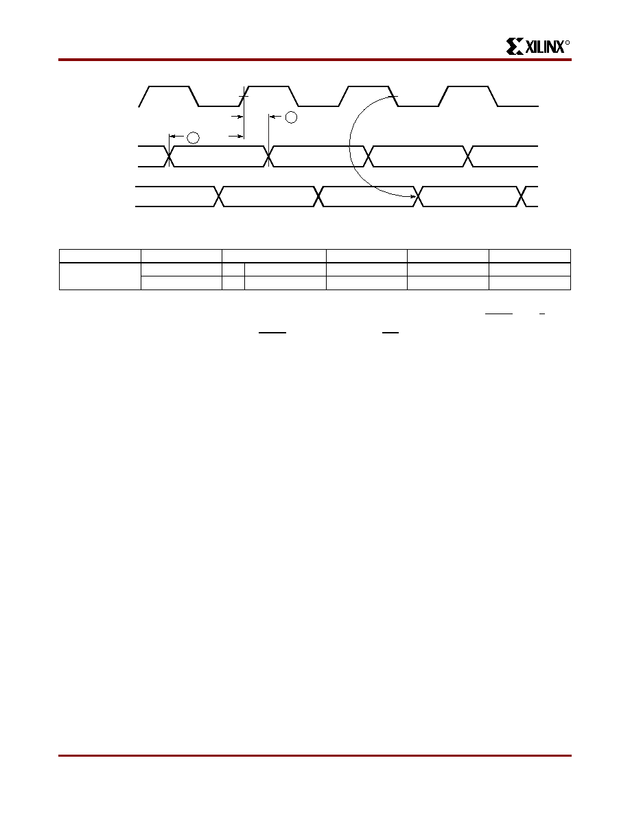
Figure 24: Master Serial Mode Programming Switching Characteristics
Serial Data In
CCLK
(Output)
Serial DOUT
(Output)
1
TDSCK
2
TCKDS
n
n + 1
n + 2
n – 3
n – 2
n – 1
n
X3223
Description
Symbol
Min
Max
Units
CCLK
Data In setup
1
TDSCK
60
ns
Data In hold
2
CKDS
0ns
Product Obsolete or Under Obsolescence
相關(guān)PDF資料 |
PDF描述 |
|---|---|
| ASM43DTMI | CONN EDGECARD 86POS R/A .156 SLD |
| ASM43DTBI | CONN EDGECARD 86POS R/A .156 SLD |
| XC3030L-8VQ64C | IC FPGA C-TEMP 3.3V 64-VQFP |
| XC2S30-5PQ208I | IC FPGA 2.5V I-TEMP 208-PQFP |
| XC2S30-5PQ208C | IC FPGA 2.5V 216 CLB'S 208-PQFP |
相關(guān)代理商/技術(shù)參數(shù) |
參數(shù)描述 |
|---|---|
| XC3042 | 制造商:Xilinx 功能描述: |
| XC3042-100CB100B | 制造商:未知廠家 制造商全稱:未知廠家 功能描述:Field Programmable Gate Array (FPGA) |
| XC3042-100CB100C | 制造商:未知廠家 制造商全稱:未知廠家 功能描述:Field Programmable Gate Array (FPGA) |
| XC3042-100CB100M | 制造商:未知廠家 制造商全稱:未知廠家 功能描述:Field Programmable Gate Array (FPGA) |
| XC3042-100CQ100C | 制造商:未知廠家 制造商全稱:未知廠家 功能描述:Field Programmable Gate Array (FPGA) |
發(fā)布緊急采購,3分鐘左右您將得到回復。