- 您現(xiàn)在的位置:買賣IC網(wǎng) > PDF目錄4174 > XC5202-6PQ100C (Xilinx Inc)IC FPGA 64 CLB'S 100-PQFP PDF資料下載
參數(shù)資料
| 型號: | XC5202-6PQ100C |
| 廠商: | Xilinx Inc |
| 文件頁數(shù): | 30/73頁 |
| 文件大小: | 0K |
| 描述: | IC FPGA 64 CLB'S 100-PQFP |
| 產(chǎn)品變化通告: | XC1700 PROMs,XC5200,HQ,SCD Parts Discontinuation 19/Jul/2010 |
| 標(biāo)準(zhǔn)包裝: | 66 |
| 系列: | XC5200 |
| LAB/CLB數(shù): | 64 |
| 邏輯元件/單元數(shù): | 256 |
| 輸入/輸出數(shù): | 81 |
| 門數(shù): | 3000 |
| 電源電壓: | 4.75 V ~ 5.25 V |
| 安裝類型: | 表面貼裝 |
| 工作溫度: | 0°C ~ 85°C |
| 封裝/外殼: | 100-BQFP |
| 供應(yīng)商設(shè)備封裝: | 100-QFP(14x20) |
| 其它名稱: | 122-1132 |
第1頁第2頁第3頁第4頁第5頁第6頁第7頁第8頁第9頁第10頁第11頁第12頁第13頁第14頁第15頁第16頁第17頁第18頁第19頁第20頁第21頁第22頁第23頁第24頁第25頁第26頁第27頁第28頁第29頁當(dāng)前第30頁第31頁第32頁第33頁第34頁第35頁第36頁第37頁第38頁第39頁第40頁第41頁第42頁第43頁第44頁第45頁第46頁第47頁第48頁第49頁第50頁第51頁第52頁第53頁第54頁第55頁第56頁第57頁第58頁第59頁第60頁第61頁第62頁第63頁第64頁第65頁第66頁第67頁第68頁第69頁第70頁第71頁第72頁第73頁
R
XC5200 Series Field Programmable Gate Arrays
7-118
November 5, 1998 (Version 5.2)
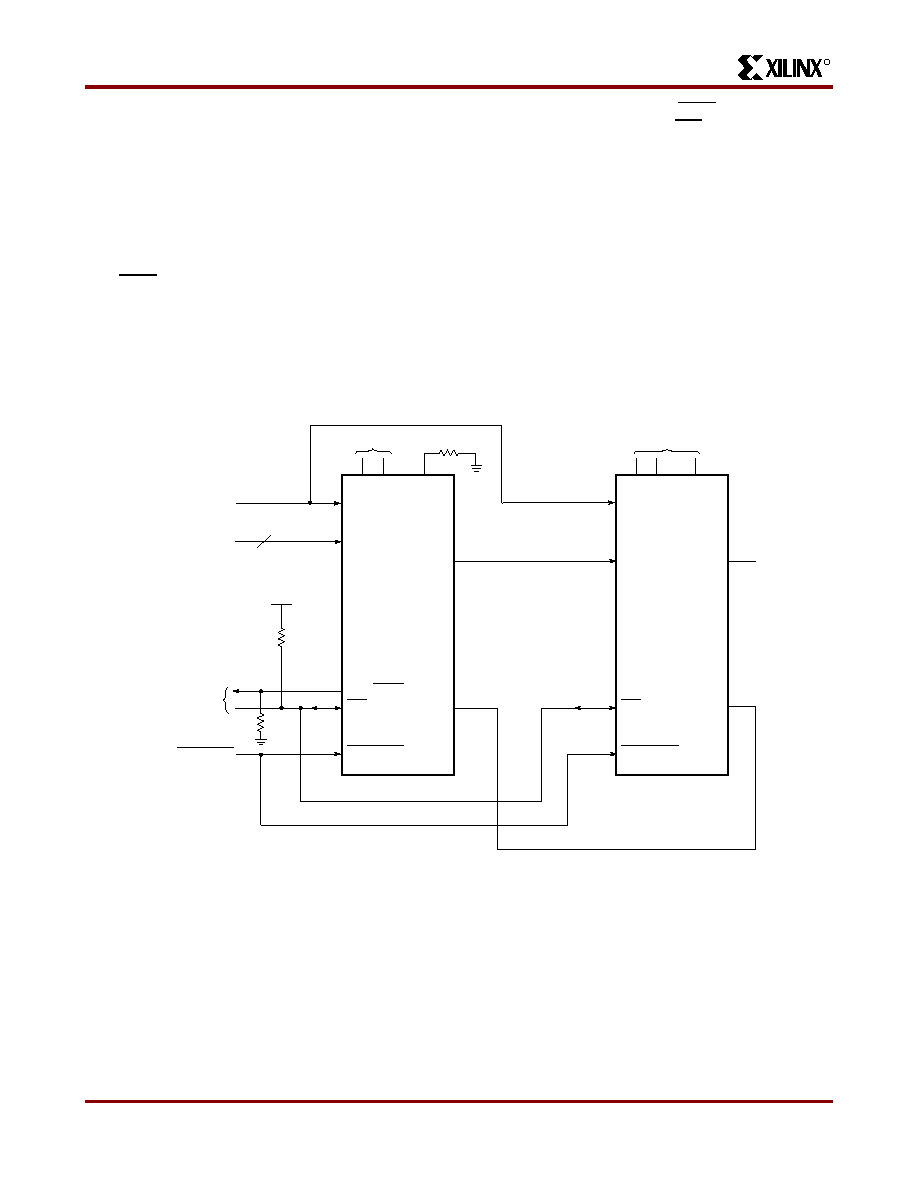
Synchronous Peripheral Mode
Synchronous Peripheral mode can also be considered
Slave Parallel mode. An external signal drives the CCLK
input(s) of the FPGA(s). The first byte of parallel configura-
tion data must be available at the Data inputs of the lead
FPGA a short setup time before the rising CCLK edge.
Subsequent data bytes are clocked in on every eighth con-
secutive rising CCLK edge.
The same CCLK edge that accepts data, also causes the
RDY/BUSY output to go High for one CCLK period. The pin
name is a misnomer. In Synchronous Peripheral mode it is
really an ACKNOWLEDGE signal. Synchronous operation
does not require this response, but it is a meaningful signal
for test purposes. Note that RDY/BUSY is pulled High with
a high-impedance pullup prior to INIT going High.
The lead FPGA serializes the data and presents the pre-
amble data (and all data that overflows the lead device) on
its DOUT pin. There is an internal delay of 1.5 CCLK peri-
ods, which means that DOUT changes on the falling CCLK
edge, and the next FPGA in the daisy chain accepts data
on the subsequent rising CCLK edge.
In order to complete the serial shift operation, 10 additional
CCLK rising edges are required after the last data byte has
been loaded, plus one more CCLK cycle for each
daisy-chained device.
Synchronous Peripheral mode is selected by a <011> on
the mode pins (M2, M1, M0).
X9005
CONTROL
SIGNALS
DATA BUS
PROGRAM
DOUT
M0 M1
M2
D0-7
INIT
DONE
PROGRAM
4.7 k
3.3 k
3.3 k
RDY/BUSY
VCC
OPTIONAL
DAISY-CHAINED
FPGAs
NOTE:
M2 can be shorted to Ground
if not used as I/O
CCLK
CLOCK
PROGRAM
DOUT
XC5200E/EX
SLAVE
M0 M1
N/C
8
M2
DIN
INIT
DONE
CCLK
N/C
XC5200
SYNCHRO-
NOUS
PERIPHERAL
Figure 33: Synchronous Peripheral Mode Circuit Diagram
Product Obsolete or Under Obsolescence
相關(guān)PDF資料 |
PDF描述 |
|---|---|
| A1225A-1PQG100C | IC FPGA 2500 GATES 100-PQFP COM |
| A1225A-PQ100I | IC FPGA 2500 GATES 100-PQFP IND |
| HMC65DRES-S93 | CONN EDGECARD 130PS .100 EYELET |
| FMC31DRXN | CONN EDGECARD 62POS DIP .100 SLD |
| XC5202-6PC84C | IC FPGA 64 CLB'S 84-PLCC |
相關(guān)代理商/技術(shù)參數(shù) |
參數(shù)描述 |
|---|---|
| XC5202-6PQ100C0100 | 制造商:Xilinx 功能描述: |
| XC5202-6PQ100I | 制造商:未知廠家 制造商全稱:未知廠家 功能描述:Field Programmable Gate Array (FPGA) |
| XC5202-6PQ160C | 制造商:XILINX 制造商全稱:XILINX 功能描述:Field Programmable Gate Arrays |
| XC5202-6PQ208C | 制造商:XILINX 制造商全稱:XILINX 功能描述:Field Programmable Gate Arrays |
| XC5202-6PQ240C | 制造商:XILINX 制造商全稱:XILINX 功能描述:Field Programmable Gate Arrays |
發(fā)布緊急采購,3分鐘左右您將得到回復(fù)。