- 您現(xiàn)在的位置:買賣IC網(wǎng) > PDF目錄372927 > XQ4010E-3PG191N (Xilinx, Inc.) QPRO XQ4000E/EX QML High-Reliability FPGAs PDF資料下載
參數(shù)資料
| 型號: | XQ4010E-3PG191N |
| 廠商: | Xilinx, Inc. |
| 元件分類: | FPGA |
| 英文描述: | QPRO XQ4000E/EX QML High-Reliability FPGAs |
| 中文描述: | QPRO XQ4000E/EX QML第高可靠性的FPGA |
| 文件頁數(shù): | 21/36頁 |
| 文件大小: | 304K |
| 代理商: | XQ4010E-3PG191N |
第1頁第2頁第3頁第4頁第5頁第6頁第7頁第8頁第9頁第10頁第11頁第12頁第13頁第14頁第15頁第16頁第17頁第18頁第19頁第20頁當(dāng)前第21頁第22頁第23頁第24頁第25頁第26頁第27頁第28頁第29頁第30頁第31頁第32頁第33頁第34頁第35頁第36頁
QPRO XQ4000E/EX QML High-Reliability FPGAs
DS021 (v2.2) June 25, 2000
Product Specification
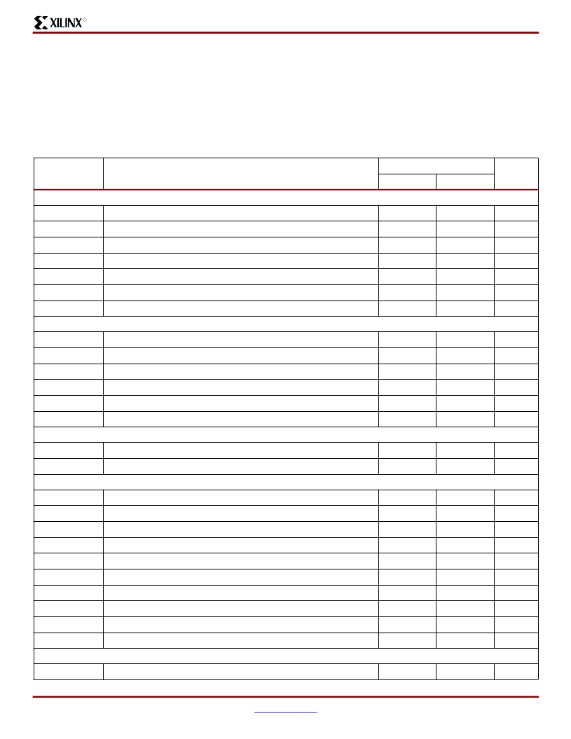
1-800-255-7778XQ4028EX CLB Switching Characteristic Guidelines
Testing of switching parameters is modeled after testing
methods specified by MIL-M-38510/605. All devices are
100% functionally tested. Internal timing parameters are
derived from measuring internal test patterns. Listed below
are representative values. For more specific, more precise,
and worst-case guaranteed data, use the values reported
by the static timing analyzer (TRCE in the Xilinx Develop-
ment System)
and back-annotated to the simulation netlist.
All timing parameters assume worst-case operating condi-
tions (supply voltage and junction temperature). Values
apply to all XQ4000EX devices unless otherwise noted.
CLB Switching Characteristics
Symbol
Description
-4
Units
Min
Max
Combinatorial Delays
T
ILO
T
IHO
T
ITO
T
HH0O
T
HH1O
T
HH2O
T
CBYP
F/G inputs to X/Y outputs
-
2.2
ns
F/G inputs via H
’
to X/Y outputs
-
3.8
ns
F/G inputs via transparent latch to Q outputs
-
3.2
ns
C inputs via SR/H0 via H to X/Y outputs
-
3.6
ns
C inputs via H1 via H to X/Y outputs
-
3.0
ns
C inputs via DIN/H2 via H to X/Y outputs
-
3.6
ns
C inputs via EC, DIN/H2 to YQ, XQ output (bypass)
-
2.0
ns
CLB Fast Carry Logic
T
OPCY
T
ASCY
T
INCY
T
SUM
T
BYP
T
NET
Operand inputs (F1, F2, G1, G4) to C
OUT
Add/Subtract input (F3) to C
OUT
Initialization inputs (F1, F3) to C
OUT
C
IN
through function generators to X/Y outputs
C
IN
to C
OUT
, bypass function generators
Carry net selay, C
OUT
to C
IN
Sequential Delays
-
2.5
ns
-
4.1
ns
-
1.9
ns
-
3.0
ns
-
0.60
ns
-
0.18
ns
T
CKO
T
CKLO
Clock K to flip-flop outputs Q
-
2.2
ns
Clock K to latch outputs Q
-
2.2
ns
Setup Time before Clock K
T
ICK
T
IHCK
T
HH0CK
T
HH1CK
T
HH2CK
T
DICK
T
ECCK
T
RCK
T
CCK
T
CHCK
Hold Time after Clock K
F/G inputs
1.3
-
ns
F/G inputs via H
3.0
-
ns
C inputs via H0 through H
2.8
-
ns
C inputs via H1 through H
2.2
-
ns
C inputs via H2 through H
2.8
-
ns
C inputs via DIN
1.2
-
ns
C inputs via EC
1.2
-
ns
C inputs via S/R, going Low (inactive)
0.8
-
ns
CIN input via F/G
2.2
-
ns
CIN input via F/G and H
3.9
-
ns
T
CKI
F/G inputs
0
-
ns
相關(guān)PDF資料 |
PDF描述 |
|---|---|
| XQ4010E-4BG191M | QPRO XQ4000E/EX QML High-Reliability FPGAs |
| XQ4010E-4BG191N | QPRO XQ4000E/EX QML High-Reliability FPGAs |
| XQ4010E-4CB191M | QPRO XQ4000E/EX QML High-Reliability FPGAs |
| XQ4010E-4CB191N | QPRO XQ4000E/EX QML High-Reliability FPGAs |
| XQ4010E-4CB196M | QPRO XQ4000E/EX QML High-Reliability FPGAs |
相關(guān)代理商/技術(shù)參數(shù) |
參數(shù)描述 |
|---|---|
| XQ4010E-3PG196M | 制造商:XILINX 制造商全稱:XILINX 功能描述:QML High-Reliability FPGAs |
| XQ4010E-3PG196N | 制造商:XILINX 制造商全稱:XILINX 功能描述:QML High-Reliability FPGAs |
| XQ4010E-4BG191M | 制造商:XILINX 制造商全稱:XILINX 功能描述:QPRO XQ4000E/EX QML High-Reliability FPGAs |
| XQ4010E-4BG191N | 制造商:XILINX 制造商全稱:XILINX 功能描述:QPRO XQ4000E/EX QML High-Reliability FPGAs |
| XQ4010E-4BG196M | 制造商:XILINX 制造商全稱:XILINX 功能描述:QML High-Reliability FPGAs |
發(fā)布緊急采購,3分鐘左右您將得到回復(fù)。