- 您現(xiàn)在的位置:買(mǎi)賣(mài)IC網(wǎng) > PDF目錄372930 > XQ4036XL-3PG411M Field Programmable Gate Array (FPGA) PDF資料下載
參數(shù)資料
| 型號(hào): | XQ4036XL-3PG411M |
| 英文描述: | Field Programmable Gate Array (FPGA) |
| 中文描述: | 現(xiàn)場(chǎng)可編程門(mén)陣列(FPGA) |
| 文件頁(yè)數(shù): | 13/22頁(yè) |
| 文件大小: | 219K |
| 代理商: | XQ4036XL-3PG411M |
第1頁(yè)第2頁(yè)第3頁(yè)第4頁(yè)第5頁(yè)第6頁(yè)第7頁(yè)第8頁(yè)第9頁(yè)第10頁(yè)第11頁(yè)第12頁(yè)當(dāng)前第13頁(yè)第14頁(yè)第15頁(yè)第16頁(yè)第17頁(yè)第18頁(yè)第19頁(yè)第20頁(yè)第21頁(yè)第22頁(yè)
QPRO XQ4000XL Series QML High-Reliability FPGAs
DS029 (v1.3) June 25, 2000
Powered by ICminer.com Electronic-Library Service CopyRight 2003
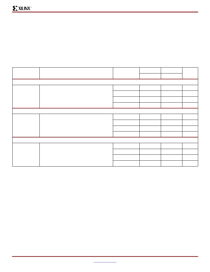
1-800-255-7778XQ4000XL Pin-to-Pin Input Parameter Guidelines
Testing of switching parameters is modeled after testing
methods specified by MIL-M-38510/605. All devices are
100% functionally tested. Pin-to-pin timing parameters are
derived from measuring external and internal test patterns
and are guaranteed over worst-case operating conditions
(supply voltage and junction temperature). Listed below are
representative values for typical pin locations and normal
clock loading. For more specific, more precise, and
worst-case guaranteed data, reflecting the actual routing
structure, use the values provided by the static timing ana-
lyzer (TRCE in the Xilinx Development System) and
back-annotated to the simulation netlist. These path delays,
provided as a guideline, have been extracted from the static
timing analyzer report. Values are expressed in nanosec-
onds unless otherwise noted.
Global Low Skew Clock, Input Setup and Hold Times
(1,2)
Symbol
Description
Device
(1)
-3
-1
Units
Min
Min
No Delay
T
PSN
/T
PHN
Global early clock and IFF
(3)
Global early clock and FCL
(4)
XQ4013XL
1.2 / 3.2
-
ns
XQ4036XL
1.2 / 5.5
-
ns
XQ4062XL
1.2 / 7.0
-
ns
XQ4085XL
-
0.9 / 7.1
ns
Partial Delay
T
PSP
/T
PHP
Global early clock and IFF
(3)
Global early clock and FCL
(4)
XQ4013XL
6.1 / 0.0
-
ns
XQ4036XL
6.4 / 1.0
-
ns
XQ4062XL
6.7 / 1.2
-
ns
XQ4085XL
-
9.8 / 1.2
ns
Full Delay
T
PSD
/T
PHD
Global early clock and IFF
(3)
XQ4013XL
6.4 / 0.0
-
ns
XQ4036XL
6.6 / 0.0
-
ns
XQ4062XL
6.8 / 0.0
-
ns
XQ4085XL
-
9.6 / 0.0
ns
Notes:
1.
2.
The XQ4013XL, XQ4036XL, and XQ4062XL have significantly faster partial and full delay setup times than other devices.
Input setup time is measured with the fastest route and the lightest load. Input hold time is measured using the furthest distance and
a reference load of one clock pin per IOB as well as driving all accessible CLB flip-flops. For designs with a smaller number of clock
loads, the pad-to-IOB clock pin delay as determined by the static timing analyzer (TRCE) can be used as a worst-case pin-to-pin
no-delay input hold specification.
IFF = Input Flip-Flop or Latch
FCL = Fast Capture Latch
3.
4.
相關(guān)PDF資料 |
PDF描述 |
|---|---|
| XQR1701LSERIES | QPro Series Configuration PROMs (XQ) including Radiation-Hardened Series (XQR) |
| XQ1701L-CC44B | Configuration EPROM |
| XQ1701L-CC44M | Configuration EPROM |
| XQ1701LSERIES | QPro Series Configuration PROMs (XQ) including Radiation-Hardened Series (XQR) |
| XQ1701L-SO20N | Configuration EPROM |
相關(guān)代理商/技術(shù)參數(shù) |
參數(shù)描述 |
|---|---|
| XQ4036XL-3PG432M | 制造商:XILINX 制造商全稱(chēng):XILINX 功能描述:QML High-Reliability FPGAs |
| XQ4036XL-3PG432N | 制造商:XILINX 制造商全稱(chēng):XILINX 功能描述:QML High-Reliability FPGAs |
| XQ4036XL-3PG475M | 制造商:XILINX 制造商全稱(chēng):XILINX 功能描述:QML High-Reliability FPGAs |
| XQ4036XL-3PG475N | 制造商:XILINX 制造商全稱(chēng):XILINX 功能描述:QML High-Reliability FPGAs |
| XQ4036XL-3PQ228M | 制造商:XILINX 制造商全稱(chēng):XILINX 功能描述:QML High-Reliability FPGAs |
發(fā)布緊急采購(gòu),3分鐘左右您將得到回復(fù)。