- 您現(xiàn)在的位置:買賣IC網(wǎng) > PDF目錄372930 > XQR4000XL QPRO XQR4000XL Radiation Hardened FPGAs PDF資料下載
參數(shù)資料
| 型號(hào): | XQR4000XL |
| 英文描述: | QPRO XQR4000XL Radiation Hardened FPGAs |
| 中文描述: | QPRO XQR4000XL抗輻射FPGA的 |
| 文件頁(yè)數(shù): | 8/20頁(yè) |
| 文件大小: | 201K |
| 代理商: | XQR4000XL |
第1頁(yè)第2頁(yè)第3頁(yè)第4頁(yè)第5頁(yè)第6頁(yè)第7頁(yè)當(dāng)前第8頁(yè)第9頁(yè)第10頁(yè)第11頁(yè)第12頁(yè)第13頁(yè)第14頁(yè)第15頁(yè)第16頁(yè)第17頁(yè)第18頁(yè)第19頁(yè)第20頁(yè)
R
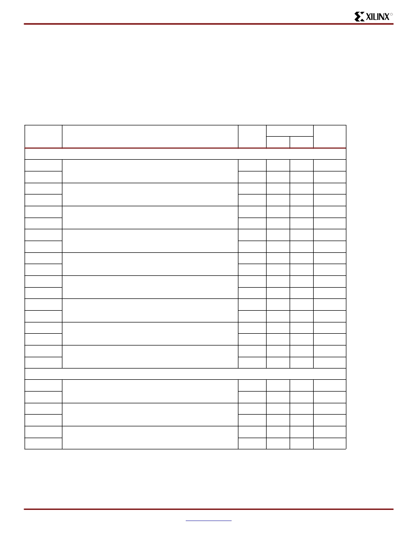
XQR4000XL RAM Synchronous (Edge-Triggered) Write Operation Guidelines
Testing of switching parameters is modeled after testing
methods specified by MIL-M-38510/605. All devices are
100% functionally tested. Internal timing parameters are
derived from measuring internal test patterns. Listed below
are representative values. For more specific, more precise,
and worst-case guaranteed data, use the values reported
by the static timing analyzer (TRCE in the Xilinx Develop-
ment System) and back-annotated to the simulation netlist.
All timing parameters assume worst-case operating condi-
tions (supply voltage and junction temperature). Values
apply to all XQR4000XL devices and are expressed in
nanoseconds unless otherwise noted.
Single-Port RAM Synchronous (Edge-Triggered) Write Operation Characteristics
Symbol
Single Port RAM
Size
-3
Units
Min
Max
Write Operation
T
WCS
T
WCTS
T
WPS
T
WPTS
T
ASS
T
ASTS
T
AHS
T
AHTS
T
DSS
T
DSTS
T
DHS
T
DHTS
T
WSS
T
WSTS
T
WHS
T
WHTS
T
WOS
T
WOTS
Read Operation
Address write cycle time (clock K period)
16x2
9.0
-
ns
32x1
9.0
-
ns
Clock K pulse width (active edge)
16x2
4.5
-
ns
32x1
4.5
-
ns
Address setup time before clock K
16x2
2.2
-
ns
32x1
2.2
-
ns
Address hold time after clock K
16x2
0
-
ns
32x1
0
-
ns
D
IN
setup time before clock K
16x2
2.0
-
ns
32x1
2.5
-
ns
D
IN
hold time after clock K
16x2
0
-
ns
32x1
0
-
ns
WE setup time before clock K
16x2
2.0
-
ns
32x1
1.8
-
ns
WE hold time after clock K
16x2
0
-
ns
32x1
0
-
ns
Data valid after clock K
16x2
-
6.8
ns
32x1
-
8.1
ns
T
RC
T
RCT
T
ILO
T
IHO
T
ICK
T
IHCK
Address read cycle time
16x2
4.5
-
ns
32x1
6.5
-
ns
Data valid after address change (no Write Enable)
16x2
-
1.6
ns
32x1
-
2.7
ns
Address setup time before clock K
16x2
1.1
-
ns
32x1
2.2
-
ns
This Material Copyrighted by Its Respective Manufacturer
相關(guān)PDF資料 |
PDF描述 |
|---|---|
| XQR4013XL-3CB228M | Field Programmable Gate Array (FPGA) |
| XQR4036XL-3CB228M | Field Programmable Gate Array (FPGA) |
| XQR4062XL-3CB228M | Field Programmable Gate Array (FPGA) |
| XR-082CP | Voltage-Feedback Operational Amplifier |
| XR-082M | Voltage-Feedback Operational Amplifier |
相關(guān)代理商/技術(shù)參數(shù) |
參數(shù)描述 |
|---|---|
| XQS14+A2FZ | 制造商:Panasonic Industrial Company 功能描述:SCREW (1/10) |
| XQS2+A5FZ | 制造商:Panasonic Industrial Company 功能描述:SCREW |
| XQS2+AJ8FZ | 制造商:Panasonic Industrial Company 功能描述:SCREW |
| XQT2LMR11D | 制造商:SunLED Group 功能描述: |
| XQT2LUG11D | 制造商:SunLED Group 功能描述: |
發(fā)布緊急采購(gòu),3分鐘左右您將得到回復(fù)。