- 您現(xiàn)在的位置:買賣IC網(wǎng) > PDF目錄16433 > XR16V698IQ-0A-EVB (Exar Corporation)EVAL BOARD FOR XR16V698-A 100QFP PDF資料下載
參數(shù)資料
| 型號(hào): | XR16V698IQ-0A-EVB |
| 廠商: | Exar Corporation |
| 文件頁(yè)數(shù): | 56/58頁(yè) |
| 文件大?。?/td> | 0K |
| 描述: | EVAL BOARD FOR XR16V698-A 100QFP |
| 標(biāo)準(zhǔn)包裝: | 1 |
| 系列: | * |
第1頁(yè)第2頁(yè)第3頁(yè)第4頁(yè)第5頁(yè)第6頁(yè)第7頁(yè)第8頁(yè)第9頁(yè)第10頁(yè)第11頁(yè)第12頁(yè)第13頁(yè)第14頁(yè)第15頁(yè)第16頁(yè)第17頁(yè)第18頁(yè)第19頁(yè)第20頁(yè)第21頁(yè)第22頁(yè)第23頁(yè)第24頁(yè)第25頁(yè)第26頁(yè)第27頁(yè)第28頁(yè)第29頁(yè)第30頁(yè)第31頁(yè)第32頁(yè)第33頁(yè)第34頁(yè)第35頁(yè)第36頁(yè)第37頁(yè)第38頁(yè)第39頁(yè)第40頁(yè)第41頁(yè)第42頁(yè)第43頁(yè)第44頁(yè)第45頁(yè)第46頁(yè)第47頁(yè)第48頁(yè)第49頁(yè)第50頁(yè)第51頁(yè)第52頁(yè)第53頁(yè)第54頁(yè)第55頁(yè)當(dāng)前第56頁(yè)第57頁(yè)第58頁(yè)

XR16V698
7
REV. 1.0.3
2.25V TO 3.6V HIGH PERFORMANCE OCTAL UART WITH 32-BYTE FIFO
1.0
DESCRIPTION
The XR16V698 (698) integrates the functions of 8 enhanced 16550 UARTs, a general purpose 16-bit timer/
counter and an on-chip oscillator. The device configuration registers include a set of four consecutive interrupt
source registers that provides interrupt-status for all 8 UARTs, timer/counter and a sleep wake up indicator.
Each UART channel has its own 16550 UART compatible configuration register set for individual channel
control, status, and data transfer. Additionally, each UART channel has 32-byte of transmit and receive FIFOs,
automatic RTS/CTS or DTR/DSR hardware flow control with hysteresis control, automatic Xon/Xoff and special
character software flow control, programmable transmit and receive FIFO trigger levels, infrared encoder and
decoder (IrDA ver. 1.0), programmable baud rate generator with a prescaler of divide by 1 or 4, and data rate
up to 15Mbps with 4X sampling clock or 7.5Mbps with 8X sampling clock at 3.3V and 10Mbps with 4X sampling
clock or 5Mbps with 8X sampling clock at 2.5V. The XR16V598 is a 2.25-3.6V device with 5 volt tolerant inputs
(except XTAL1).
2.0
FUNCTIONAL DESCRIPTIONS
2.1
Device Reset
2.1.1
Hardware Reset
The RST# input resets the internal registers and the serial interface outputs in all 8 channels to their default
state (see Table 18). A LOW pulse of longer than 40 ns duration will be required to activate the reset function
in the device.
2.1.2
Software Reset
The internal registers of each UART can be reset by writing to the RESET register in the Device Configuration
Registers. For more details, see the RESET register description on page 29.
2.2
UART Channel Selection
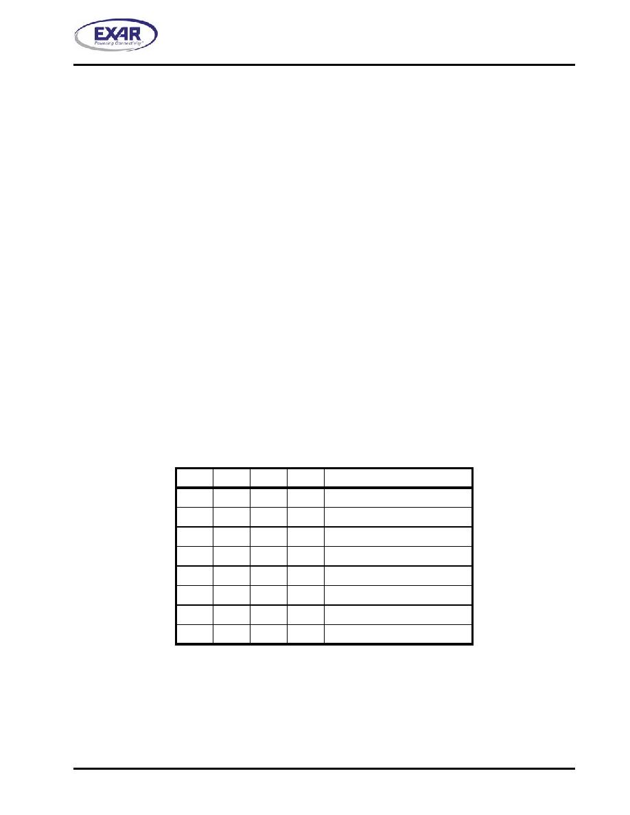
A LOW on the chip select pin, CS#, allows the user to select one of the UART channels to configure, send
transmit data and/or unload receive data to/from the UART. When address line A7 = 0, address lines A6:A4
are used to select one of the eight channels. See Table 1 below for UART channel selection.
2.3
Simultaneous Write to All Channels
During a write cycle, the setting of the Device Configuration register REGB (See Table 8) bit-0 to a logic 1 will
override the channel selection of address A6:A4 and allow a simultaneous write to all 8 UART channels when
any channel is written to. This functional capability allow the registers in all 8 UART channels to be modified
concurrently, saving individual channel initialization time. Caution should be considered, however, when using
this capability. Any in-process serial data transfer may be disrupted by changing an active channel’s mode.
TABLE 1: UART CHANNEL SELECTION
A7
A6
A5
A4
FUNCTION
0
Channel 0 Selected
0
1
Channel 1 Selected
0
1
0
Channel 2 Selected
0
1
Channel 3 Selected
0
1
0
Channel 4 Selected
0
1
0
1
Channel 5 Selected
0
1
0
Channel 6 Selected
0
1
Channel 7 Selected
相關(guān)PDF資料 |
PDF描述 |
|---|---|
| KIT33972AEWEVBE | KIT EVALUATION FOR MC33972 |
| EBM31DCMS | CONN EDGECARD 62POS .156 WW |
| VI-J1L-EX | CONVERTER MOD DC/DC 28V 75W |
| XR16V598IQ-0B-EVB | EVAL BOARD FOR XR16V598-A 100QFP |
| CM322522-820KL | INDUCTOR 82UH 60MA SMD |
相關(guān)代理商/技術(shù)參數(shù) |
參數(shù)描述 |
|---|---|
| XR16V698IQ-0B-EVB | 功能描述:UART 接口集成電路 Supports V698 100 ld QFP, PCI Interface RoHS:否 制造商:Texas Instruments 通道數(shù)量:2 數(shù)據(jù)速率:3 Mbps 電源電壓-最大:3.6 V 電源電壓-最小:2.7 V 電源電流:20 mA 最大工作溫度:+ 85 C 最小工作溫度:- 40 C 封裝 / 箱體:LQFP-48 封裝:Reel |
| XR16V698IQ100 | 制造商:EXAR 制造商全稱:EXAR 功能描述:2.25V TO 3.6V HIGH PERFORMANCE OCTAL UART WITH 32-BYTE FIFO |
| XR16V698IQ100-F | 功能描述:UART 接口集成電路 UART RoHS:否 制造商:Texas Instruments 通道數(shù)量:2 數(shù)據(jù)速率:3 Mbps 電源電壓-最大:3.6 V 電源電壓-最小:2.7 V 電源電流:20 mA 最大工作溫度:+ 85 C 最小工作溫度:- 40 C 封裝 / 箱體:LQFP-48 封裝:Reel |
| XR16V698IQ100TR-F | 制造商:Exar Corporation 功能描述:UART 8-CH 32Byte FIFO 2.5V/3.3V 100-Pin PQFP T/R 制造商:Exar Corporation 功能描述:XR16V698IQ100TR-F |
| XR16V794 | 制造商:EXAR 制造商全稱:EXAR 功能描述:HIGH PERFORMANCE 2.25V TO 3.6V QUAD UART WITH FRACTIONAL |
發(fā)布緊急采購(gòu),3分鐘左右您將得到回復(fù)。