- 您現(xiàn)在的位置:買賣IC網(wǎng) > PDF目錄376460 > XRT4500 (Exar Corporation) MULTIPROTOCOL SERIAL NETWORK INTERFACE IC PDF資料下載
參數(shù)資料
| 型號: | XRT4500 |
| 廠商: | Exar Corporation |
| 英文描述: | MULTIPROTOCOL SERIAL NETWORK INTERFACE IC |
| 中文描述: | 多協(xié)議串行網(wǎng)絡(luò)接口芯片 |
| 文件頁數(shù): | 51/99頁 |
| 文件大小: | 1384K |
| 代理商: | XRT4500 |
第1頁第2頁第3頁第4頁第5頁第6頁第7頁第8頁第9頁第10頁第11頁第12頁第13頁第14頁第15頁第16頁第17頁第18頁第19頁第20頁第21頁第22頁第23頁第24頁第25頁第26頁第27頁第28頁第29頁第30頁第31頁第32頁第33頁第34頁第35頁第36頁第37頁第38頁第39頁第40頁第41頁第42頁第43頁第44頁第45頁第46頁第47頁第48頁第49頁第50頁當前第51頁第52頁第53頁第54頁第55頁第56頁第57頁第58頁第59頁第60頁第61頁第62頁第63頁第64頁第65頁第66頁第67頁第68頁第69頁第70頁第71頁第72頁第73頁第74頁第75頁第76頁第77頁第78頁第79頁第80頁第81頁第82頁第83頁第84頁第85頁第86頁第87頁第88頁第89頁第90頁第91頁第92頁第93頁第94頁第95頁第96頁第97頁第98頁第99頁

XRT4500
MULTIPROTOCOL SERIAL NETWORK INTERFACE IC
REV. 1.0.7
á
48
2. The Analog/Line-Side Loop-back path:
This loop-back path is referred to as an “Analog/Line-
Side” Loop-back, because all signals originate from and
are ultimately terminated by the DCE Terminal. These
signals originate from the DCE Terminal; and are out-
putted to the line, to the DTE Terminal. However, these
signals (from the DCE Terminal) are never converted in-
to the Digital format (by the DTE Mode XRT4500).
These signal are kept in the “Analog” format, and are
looped-back (over the line) to the DCE Terminal.
The RXD signal (originating from the DCE Terminal)
will be transmitted over the line to the DTE Terminal.
However, this signal will not be converted into the dig-
ital format by the “DTE Mode” XRT4500. Instead, this
signal will be looped-back out to the “DCE Terminal”
via the “TXD” signal path.
N
OTE
:
In this loop-back mode, the RXC signal (e.g., the
companion clock signal to RXD) is also received by the
DTE Terminal and looped-back out to the DCE Terminal. In
this case, the “RXC” (Receive Clock) signal will be routed to
the DCE Terminal through the “SCTE” signal path The DCE
SCC can still use the RXC (via the SCTE signal path), in
order to sample the RXD signal (which is available via the
“TXD” signal path).
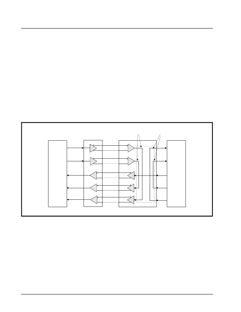
Behavior of the DCE Mode XRT4500, when the
Loop-Back Mode is Enabled.
Figure 19 presents an illustration of a DTE and a
DCE Terminal interfaced to each other. In this case,
the XRT4500 (associated with the DCE Terminal) has
been configured to operate in the “Loop-back” Mode.
N
OTE
:
Figure 19 only depicts the “High-Speed” DCE/DTE
Interface signals. The “Low-Speed” control/handshaking
signals are not affected by the loop-back mode.
If the Loop-back Mode is configured within the
XRT4500, while it is operating in the DCE Mode, then
the following two (2) loop-back paths exists.
A Digital/Terminal-Side Loop-back
An Analog/Line-Side Loop-back
Each of these Loop-back paths are described below.
1. The Digital/Terminal Side Loop-back:
Again, this loop-back path is referred to as a “Digital/
Terminal Side” Loop-back, because all of the signals
originate from, and are terminated by the DCE SCC
(e.g., the Terminal Equipment). The signals (originat-
ing at the DCE SCC) are not converted into the Ana-
log format, and are not output to the line.
The “RXD” signal (originating from the DCE SCC)
along with the “RXC” (Receive Clock) signal will not
be converted into the Analog format, nor output to the
DTE Terminal (over the line). Instead, this signal will
remain in the “Digital-format” and will be looped-back
into the DCE SCC. The “RXD” signal will ultimately be
output to the DCE SCC via the “TXD” output of the
“DCE Mode” XRT4500.
N
OTE
:
The “RXC” signal (e.g., the companion clock signal to
“RXD”) will also be loop-back into the “DCE SCC”. This signal
will be output (by the XRT4500) via the “SCTE” output pin.
F
IGURE
19. I
LLUSTRATION
OF
THE
B
EHAVIOR
OF
THE
DCE M
ODE
XRT4500,
WHEN
IT
IS
CONFIGURED
TO
OPERATE
IN
THE
L
OOP
-
BACK
M
ODE
SCC (R)
SCC (L)
XRT4500
XRT4500
RX1
TX1
RX2
TX2
RX3
TX3
RX2
TX2
RX1
TX1
RXD
RXC
TXC
SCTE_IN
TXD_IN
TXD
SCTE
TXC_IN
RXC_IN
RXD_IN
60
67
73
74
1
78
79
77
76
70
71
64
65
63
62
1
74
68
67
60
63
62
64
65
70
71
77
76
78
79
TXD
SCTE
TXC
RXC
RXD
Analog/Line
Loop-back Path
Digital/Terminal
Loop-back Path
DTE (#1)
DCE (#4)
MUX 1
相關(guān)PDF資料 |
PDF描述 |
|---|---|
| XRT4500CV | MULTIPROTOCOL SERIAL NETWORK INTERFACE IC |
| XRT56L85 | Low Power PCM Line Interface |
| XRT5794ES | Evaluation System |
| XRT5894ES | () |
| XRT5894 | Four-Channel E1 Line Interface (3.3V or 5.0V)(四通道E1 3.3V線接口單元) |
相關(guān)代理商/技術(shù)參數(shù) |
參數(shù)描述 |
|---|---|
| XRT4500CV | 制造商:EXAR 制造商全稱:EXAR 功能描述:MULTIPROTOCOL SERIAL NETWORK INTERFACE IC |
| XR-T5600P | 制造商:未知廠家 制造商全稱:未知廠家 功能描述:PCM Repeater |
| XR-T56188CD | 制造商:未知廠家 制造商全稱:未知廠家 功能描述:PCM Transceiver |
| XR-T56188CP | 制造商:未知廠家 制造商全稱:未知廠家 功能描述:PCM Transceiver |
| XR-T56188ID | 制造商:未知廠家 制造商全稱:未知廠家 功能描述:PCM Transceiver |
發(fā)布緊急采購,3分鐘左右您將得到回復。