- 您現(xiàn)在的位置:買賣IC網(wǎng) > PDF目錄376461 > XRT73L06IB (EXAR CORP) SIX CHANNEL E3/DS3/STS-1 LINE INTERFACE UNIT PDF資料下載
參數(shù)資料
| 型號: | XRT73L06IB |
| 廠商: | EXAR CORP |
| 元件分類: | 數(shù)字傳輸電路 |
| 英文描述: | SIX CHANNEL E3/DS3/STS-1 LINE INTERFACE UNIT |
| 中文描述: | DATACOM, PCM TRANSCEIVER, PBGA217 |
| 封裝: | 23 X 23 MM, BGA-217 |
| 文件頁數(shù): | 21/63頁 |
| 文件大?。?/td> | 348K |
| 代理商: | XRT73L06IB |
第1頁第2頁第3頁第4頁第5頁第6頁第7頁第8頁第9頁第10頁第11頁第12頁第13頁第14頁第15頁第16頁第17頁第18頁第19頁第20頁當(dāng)前第21頁第22頁第23頁第24頁第25頁第26頁第27頁第28頁第29頁第30頁第31頁第32頁第33頁第34頁第35頁第36頁第37頁第38頁第39頁第40頁第41頁第42頁第43頁第44頁第45頁第46頁第47頁第48頁第49頁第50頁第51頁第52頁第53頁第54頁第55頁第56頁第57頁第58頁第59頁第60頁第61頁第62頁第63頁

XRT73L06
REV. 1.0.2
SIX CHANNEL E3/DS3/STS-1 LINE INTERFACE UNIT
18
2.2
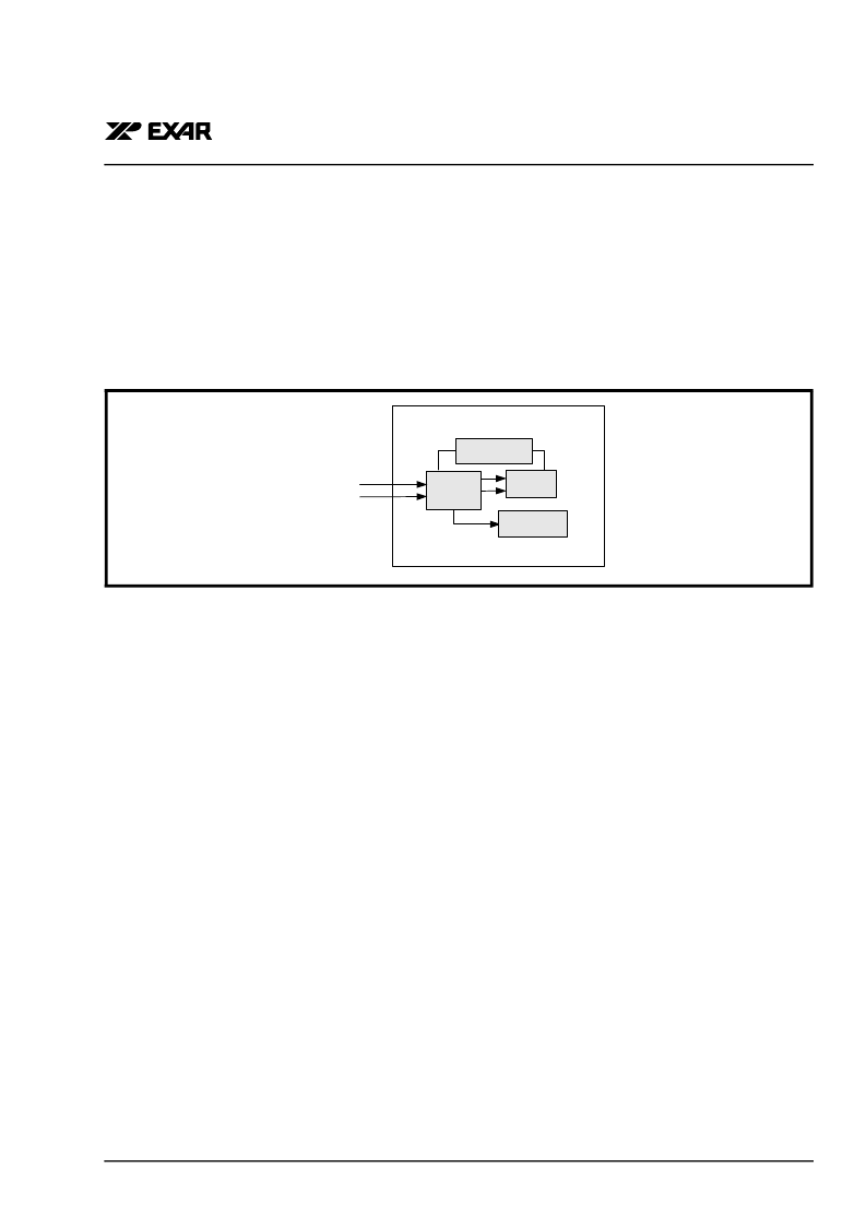
The Adaptive Gain Control circuit amplifies the incoming analog signal and compensates for the various flat
losses and also for the loss at one-half symbol rate. The AGC has a dynamic range of 30 dB. The peak
detector provides feedback to the equalizer before slicing occurs.
2.3
Receive Equalizer
The Equalizer restores the integrity of the signal and compensates for the frequency dependent attenuation of
up to 900 feet of coaxial cable (1300 feet for E3). The Equalizer also boosts the high frequency content of the
signal to reduce Inter-Symbol Interference (ISI) so that the slicer slices the signal at 50% of peak voltage to
generate Positive and Negative data. The equalizer can be disabled by programming the appropriate register.
Adaptive Gain Control (AGC)
F
IGURE
7. ACG/E
QUALIZER
B
LCOK
D
IAGRAM
2.3.1
The Equalizer has two gain settings to provide optimum equalization. In the case of normally shaped DS3/
STS-1 pulses (pulses that meet the template requirements) that has been driven through 0 to 900 feet of cable,
the Equalizer can be enabled. However, for square-shaped pulses such as E3 or for DS3/STS-1 high pulses
(that does not meet the pulse template requirements), it is recommended that the Equalizer be disabled for
cable length less than 300 feet. This would help to prevent over-equalization of the signal and thus optimize
the performance in terms of better jitter transfer characteristics. The Equalizer also contains an additional 20
dB gain stage to provide the line monitoring capability of the resistively attenuated signals which may have
20dB flat loss. The equalizer gain mode can be enabled by programming the appropriate register.
Recommendations for Equalizer Settings
N
OTE
:
The results of extensive testing indicate that even when the Equalizer was enabled, regardless of the cable length,
the integrity of the E3 signal was restored properly over 0 to 12 dB cable loss at Industrial Temperature.
2.4
Clock and Data Recovery
The Clock and Data Recovery Circuit extracts the embedded clock, RxClk_n from the sliced digital data stream
and provides the retimed data to the B3ZS (HDB3) decoder. The Clock Recovery PLL can be in one of the
following two modes:
2.4.1
Data/Clock Recovery Mode
In the presence of input line signals on the RTIP_n and RRing_n input pins and when the frequency difference
between the recovered clock signal and the reference clock signal is less than 0.5%, the clock that is output on
the RxClk_n out pins is the Recovered Clock signal.
2.4.2
Training Mode
In the absence of input signals at RTIP_n and RRing_n pins, or when the frequency difference between the
recovered line clock signal and the reference clock applied on the ExClk_n input pins exceed 0.5%, a Loss of
Lock condition is declared by toggling RLOL_n output pin “High” or setting the RLOL_n bit to “1” in the control
register. Also, the clock output on the RxClk_n pins are the same as the reference channel clock.
AGC/
Equalizer
Peak Detector
LOS
Detector
Slicer
RTIP_n
RRing_n
相關(guān)PDF資料 |
PDF描述 |
|---|---|
| XRT73LC00A | E3/DS3/STS-1 LINE INTERFACE UNIT |
| XRT73LC00AIV | E3/DS3/STS-1 LINE INTERFACE UNIT |
| XRT73LC03A | 3 CHANNEL DS3/E3/STS-1 LINE INTERFACE UNIT |
| XRT73LC03AIV | 3 CHANNEL DS3/E3/STS-1 LINE INTERFACE UNIT |
| XRT73LC04A | 4 CHANNEL DS3/E3/STS-1 LINE INTERFACE UNIT |
相關(guān)代理商/技術(shù)參數(shù) |
參數(shù)描述 |
|---|---|
| XRT73L06IB-F | 功能描述:接口 - 專用 RoHS:否 制造商:Texas Instruments 產(chǎn)品類型:1080p60 Image Sensor Receiver 工作電源電壓:1.8 V 電源電流:89 mA 最大功率耗散: 最大工作溫度:+ 85 C 安裝風(fēng)格:SMD/SMT 封裝 / 箱體:BGA-59 |
| XRT73L06IQ | 制造商:未知廠家 制造商全稱:未知廠家 功能描述:Telecomm/Datacomm |
| XRT73LC00 | 制造商:EXAR 制造商全稱:EXAR 功能描述:E3/DS3/STS-1 LINE INTERFACE UNIT |
| XRT73LC00A | 制造商:EXAR 制造商全稱:EXAR 功能描述:E3/DS3/STS-1 LINE INTERFACE UNIT |
| XRT73LC00A_08 | 制造商:EXAR 制造商全稱:EXAR 功能描述:E3/DS3/STS-1 LINE INTERFACE UNIT |
發(fā)布緊急采購,3分鐘左右您將得到回復(fù)。