- 您現(xiàn)在的位置:買賣IC網(wǎng) > PDF目錄373766 > Z86C34 (ZiLOG, Inc.) CMOS Z8 MCU(CMOS Z8系列微控制器) PDF資料下載
參數(shù)資料
| 型號(hào): | Z86C34 |
| 廠商: | ZiLOG, Inc. |
| 英文描述: | CMOS Z8 MCU(CMOS Z8系列微控制器) |
| 中文描述: | 單片機(jī)的CMOS Z8的CMOS(Z8系列微控制器) |
| 文件頁(yè)數(shù): | 29/70頁(yè) |
| 文件大?。?/td> | 1192K |
| 代理商: | Z86C34 |
第1頁(yè)第2頁(yè)第3頁(yè)第4頁(yè)第5頁(yè)第6頁(yè)第7頁(yè)第8頁(yè)第9頁(yè)第10頁(yè)第11頁(yè)第12頁(yè)第13頁(yè)第14頁(yè)第15頁(yè)第16頁(yè)第17頁(yè)第18頁(yè)第19頁(yè)第20頁(yè)第21頁(yè)第22頁(yè)第23頁(yè)第24頁(yè)第25頁(yè)第26頁(yè)第27頁(yè)第28頁(yè)當(dāng)前第29頁(yè)第30頁(yè)第31頁(yè)第32頁(yè)第33頁(yè)第34頁(yè)第35頁(yè)第36頁(yè)第37頁(yè)第38頁(yè)第39頁(yè)第40頁(yè)第41頁(yè)第42頁(yè)第43頁(yè)第44頁(yè)第45頁(yè)第46頁(yè)第47頁(yè)第48頁(yè)第49頁(yè)第50頁(yè)第51頁(yè)第52頁(yè)第53頁(yè)第54頁(yè)第55頁(yè)第56頁(yè)第57頁(yè)第58頁(yè)第59頁(yè)第60頁(yè)第61頁(yè)第62頁(yè)第63頁(yè)第64頁(yè)第65頁(yè)第66頁(yè)第67頁(yè)第68頁(yè)第69頁(yè)第70頁(yè)
Z86C34/C35/C36/C44/C45/C46
CMOS Z8 MCUs with ASCI UART
ZiLOG
DS007601-Z8X0499
P R E L I M I N A R Y
29
FUNCTIONAL DESCRIPTION
The Z8 MCU incorporates the following special functions
to enhance the standard Z8
architecture to provide the user
with increased design flexibility.
RESET.
The device is reset in one of the following condi-
tions:
Power-On Reset
Watch-Dog Timer
Stop-Mode Recovery Source
External Reset
Low Voltage Recovery
Auto Power-On Reset circuitry is built into the Z8, elimi-
nating the requirement for an external reset circuit to reset
upon power-up. The internal pull-up resistor is on the Reset
pin, so a pull-up resistor is not required; however, in a high-
EMI (noisy) environment, it is recommended that a small
value pull-up resistor be used.
Note:
The
RESET
pin is not available on devices in the 28-pin
package.
Program Memory.
The first 12 bytes of program memory
are reserved for the interrupt vectors. These locations con-
tain six 16-bit vectors that correspond to the six available
interrupts. For ROM mode, address 12 to address
65535
(C36/C46)/
32767
(C35/C45)/
16383
(C34/C44) consists
of on-chip mask-programmed ROM. The Z86C44/C45 can
access external program and data memory from addresses
16384/32768 to 65535.
The
65535
(C36/C46)/
32767
(C35/C45)/
16383
(C34/C44) program memory is mask programmable.
A
ROM protect feature prevents dumping of the ROM con-
tents by inhibiting execution of
LDC
,
LDCI
,
LDE
,
and
LDEI
instructions to Program Memory in external program
mode
. ROM look-up tables can be used with this feature.
The ROM Protect option is mask-programmable, to be se-
lected by the customer when the ROM code is submitted.
Data Memory (
DM
).
The ROMless version can address up
to 64 KB of external data memory. External data memory
may be included with, or separated from, the external pro-
gram memory space.
DM
, an optional I/O function that can
be programmed to appear on pin
P34
, is used to distinguish
between data and program memory space (Figure 18). The
state of the
DM
signal is controlled by the type of instruction
being executed. An
LDC
Op Code references
PROGRAM
(
DM
inactive) memory, and an
LDE
instruction references
data (
DM
active Low) memory. The user must configure
Port 3 Mode Register (
P3M
) bits
D3
and
D4
for this mode.
This feature is not usable for devices in 28-pin package.
When used in ROM mode, the Z86C46 cannot access any
external data memory.
The Z86C44/C45 can access exter-
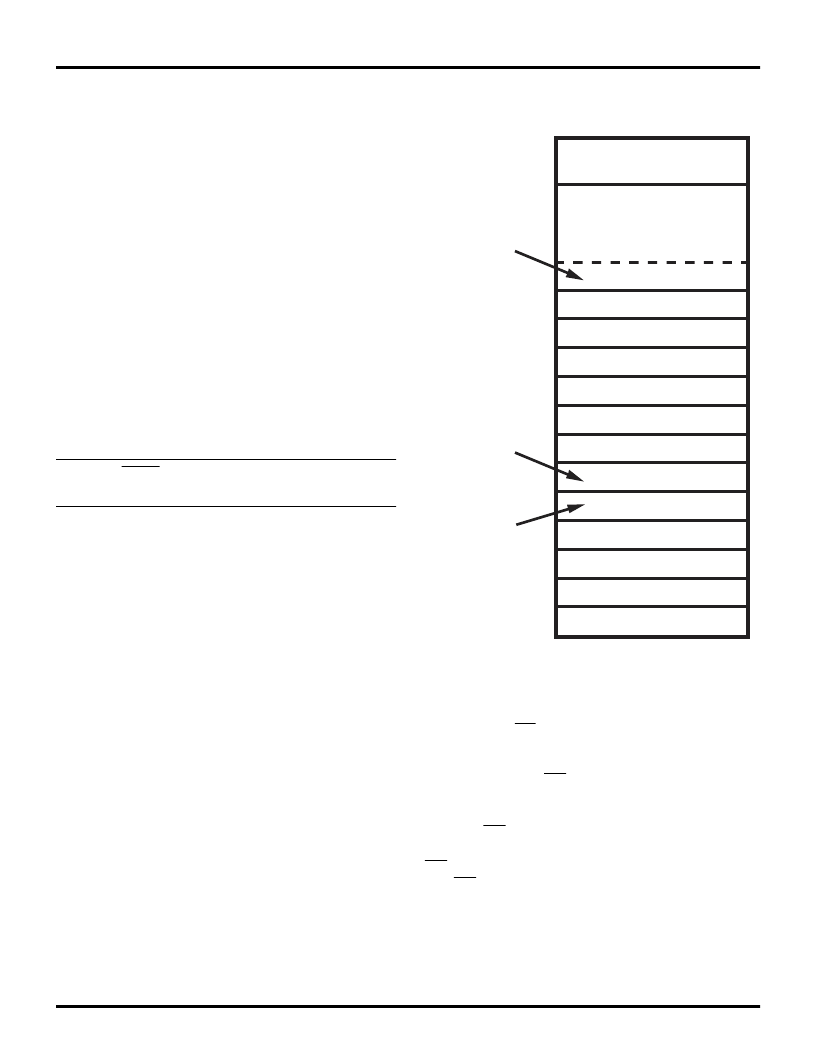
Figure 17. Program Memory Map
for Z86C34/35/44/45
12
11
10
9
8
7
6
5
4
3
2
1
0
On-Chip
ROM
Location of
First Byte of
Instruction
Executed
After RESET
Interrupt
Vector
(Lower Byte)
Interrupt
Vector
(Upper Byte)
IRQ5
IRQ4
IRQ4
IRQ3
IRQ3
IRQ2
IRQ2
IRQ1
IRQ1
IRQ0
IRQ0
IRQ5
16383/32767
16382/32766
External/Internal
ROM and RAM
65535
相關(guān)PDF資料 |
PDF描述 |
|---|---|
| Z86C35 | CMOS Z8 MCU(CMOS Z8系列微控制器) |
| Z86C36 | CMOS Z8 MCU(CMOS Z8系列微控制器) |
| Z86C44 | CMOS Z8 MCU(CMOS Z8系列微控制器) |
| Z86C45 | CMOS Z8 MCU(CMOS Z8系列微控制器) |
| Z86C46 | CMOS Z8 MCU(CMOS Z8系列微控制器) |
相關(guān)代理商/技術(shù)參數(shù) |
參數(shù)描述 |
|---|---|
| Z86C35 | 制造商:ZILOG 制造商全稱:ZILOG 功能描述:CMOS Z8 MCUs WITH ASCI UART OFFER EFFICIENT, COST-EFFECTIVE DESIGN FLEXIBILITY |
| Z86C36 | 制造商:ZILOG 制造商全稱:ZILOG 功能描述:CMOS Z8 MCUs WITH ASCI UART OFFER EFFICIENT, COST-EFFECTIVE DESIGN FLEXIBILITY |
| Z86C3600ZEM | 功能描述:仿真器/模擬器 Z8 C36 ICEBOX RoHS:否 制造商:Blackhawk 產(chǎn)品:System Trace Emulators 工具用于評(píng)估:C6000, C5000, C2000, OMAP, DAVINCI, SITARA, TMS470, TMS570, ARM 7/9, ARM Cortex A8/R4/M3 用于:XDS560v2 |
| Z86C40 | 制造商:ZILOG 制造商全稱:ZILOG 功能描述:CMOS Z8 CONSUMER CONTROLLER PROCESSOR |
| Z86C4000ZDV | 功能描述:仿真器/模擬器 Z86C40 PLCC Em Pod RoHS:否 制造商:Blackhawk 產(chǎn)品:System Trace Emulators 工具用于評(píng)估:C6000, C5000, C2000, OMAP, DAVINCI, SITARA, TMS470, TMS570, ARM 7/9, ARM Cortex A8/R4/M3 用于:XDS560v2 |
發(fā)布緊急采購(gòu),3分鐘左右您將得到回復(fù)。