- 您現(xiàn)在的位置:買賣IC網(wǎng) > PDF目錄373766 > Z86C45 (ZiLOG, Inc.) CMOS Z8 MCU(CMOS Z8系列微控制器) PDF資料下載
參數(shù)資料
| 型號: | Z86C45 |
| 廠商: | ZiLOG, Inc. |
| 英文描述: | CMOS Z8 MCU(CMOS Z8系列微控制器) |
| 中文描述: | 單片機(jī)的CMOS Z8的CMOS(Z8系列微控制器) |
| 文件頁數(shù): | 41/70頁 |
| 文件大?。?/td> | 1192K |
| 代理商: | Z86C45 |
第1頁第2頁第3頁第4頁第5頁第6頁第7頁第8頁第9頁第10頁第11頁第12頁第13頁第14頁第15頁第16頁第17頁第18頁第19頁第20頁第21頁第22頁第23頁第24頁第25頁第26頁第27頁第28頁第29頁第30頁第31頁第32頁第33頁第34頁第35頁第36頁第37頁第38頁第39頁第40頁當(dāng)前第41頁第42頁第43頁第44頁第45頁第46頁第47頁第48頁第49頁第50頁第51頁第52頁第53頁第54頁第55頁第56頁第57頁第58頁第59頁第60頁第61頁第62頁第63頁第64頁第65頁第66頁第67頁第68頁第69頁第70頁
Z86C34/C35/C36/C44/C45/C46
CMOS Z8 MCUs with ASCI UART
ZiLOG
DS007601-Z8X0499
P R E L I M I N A R Y
41
Stop-Mode Recovery Register 2 (SMR2).
This register
contains additional Stop-Mode Recovery sources. When
the Stop-Mode Recovery sources are selected in this reg-
ister then
SMR
Register. Bits
D2
,
D3
, and
D4
must be
0
.
Watch-Dog Timer Mode Register (WDTMR).
The
WDT
is a retriggerable one-shot timer that resets the Z8 if it reach-
es its terminal count. The
WDT
is initially enabled by exe-
cuting the
WDT
instruction and refreshed on subsequent ex-
ecutions of the
WDT
instruction. The
WDT
circuit is driven
by an onboard
RC
oscillator or external oscillator from the
XTAL1
pin. The
POR
clock source is selected with bit
4
of
the
WDT
register (Figure 29).
WDT
instruction affects the Z (Zero), S (Sign), and V (Over-
flow) flags. The
WDTMR
must be written to within 64 in-
ternal system clocks. After that, the
WDTMR
is
WRITE
-pro-
tected.
Note:
WDT
time-out while in
STOP
mode does not reset
SMR
,
PCON
,
WDTMR
,
P2M
,
P3M
, Ports 2 & 3 Data Registers,
but the
POR
delay counter is still enabled even though
the
SMR
stop delay is disabled.
WDT Time Select. (D0,D1).
Selects the
WDT
time period
and is configured as indicated in Table 15.
Table 14. Stop-Mode Recovery Source
SMR:10
D1 D0
Operation
Description of Action
0
0
1
0
1
0
POR and/or external reset recovery
Logical AND of P20 through P23
Logical AND of P20 through P27
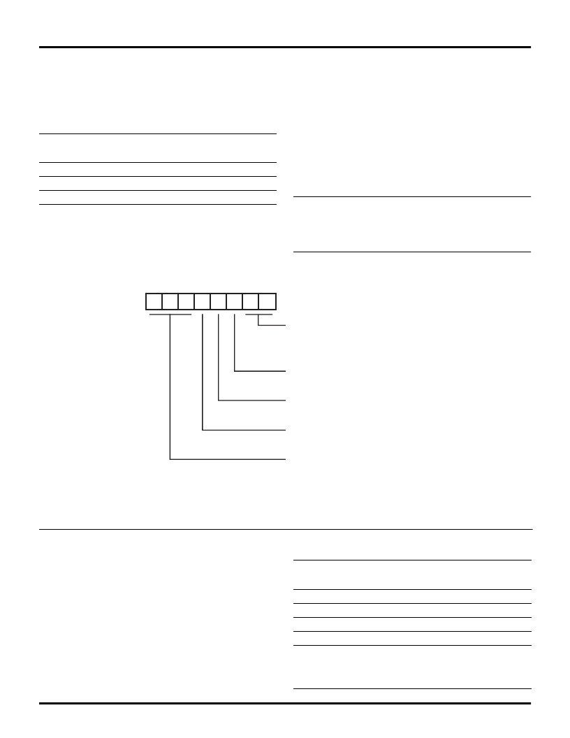
Figure 29. Watch-Dog Timer Mode Register (WRITE ONLY)
D7
D6
D5
D4
D3
D2
D1
D0
WDTMR (F) 0F
WDT TAP INT RC OSC External Clock
00 3.5 ms 128 TpC
01
*
7 ms 256 TpC
10 14 ms 512 TpC
11 56 ms 2048 TpC
WDT During HALT
0 OFF
1 ON
*
WDT During STOP
0 OFF
1 ON
*
XTAL1/INT RC Select for WDT
0 On-Board RC
*
1 XTAL
Reserved (must be 0)
*
Default setting after RESET
Table 15. WDT Time Select
D1
D0
Timeout of
Internal RC OSC
Timeout of
System Clock
0
0
1
1
0
1
0
1
3.5 ms min
7 ms min
14 ms min
56 ms min
128 SCLK
256 SCLK
512 SCLK
2048 SCLK
Notes:
SCLK = system bus clock cycle.
The default on RESET is 7 ms.
Values provided are for V
CC
= 5.0V.
相關(guān)PDF資料 |
PDF描述 |
|---|---|
| Z86C46 | CMOS Z8 MCU(CMOS Z8系列微控制器) |
| Z86C40 | CMOS Z8 CONSUMER CONTROLLER PROCESSOR |
| Z86C30 | CMOS Z8 CONSUMER CONTROLLER PROCESSOR |
| Z86C31 | CMOS Z8 CONSUMER CONTROLLER PROCESSOR |
| Z86C32 | CMOS Z8 CONSUMER CONTROLLER PROCESSOR |
相關(guān)代理商/技術(shù)參數(shù) |
參數(shù)描述 |
|---|---|
| Z86C46 | 制造商:ZILOG 制造商全稱:ZILOG 功能描述:CMOS Z8 MCUs WITH ASCI UART OFFER EFFICIENT, COST-EFFECTIVE DESIGN FLEXIBILITY |
| Z86C47 | 制造商:ZILOG 制造商全稱:ZILOG 功能描述:CMOS Z8 MICROCONTROLLER |
| Z86C4704PSC | 制造商:未知廠家 制造商全稱:未知廠家 功能描述:8-Bit Microcontroller |
| Z86C5000ZEM | 功能描述:仿真器/模擬器 Z8 In-Circuit Em-C50 RoHS:否 制造商:Blackhawk 產(chǎn)品:System Trace Emulators 工具用于評估:C6000, C5000, C2000, OMAP, DAVINCI, SITARA, TMS470, TMS570, ARM 7/9, ARM Cortex A8/R4/M3 用于:XDS560v2 |
| Z86C50-20GSE | 制造商:未知廠家 制造商全稱:未知廠家 功能描述:8-Bit Microcontroller |
發(fā)布緊急采購,3分鐘左右您將得到回復(fù)。