- 您現在的位置:買賣IC網 > PDF目錄373783 > ZL30119GGG (ZARLINK SEMICONDUCTOR INC) SONET/SDH OC-48/OC-192 Line Card Synchronizer PDF資料下載
參數資料
| 型號: | ZL30119GGG |
| 廠商: | ZARLINK SEMICONDUCTOR INC |
| 元件分類: | 數字傳輸電路 |
| 英文描述: | SONET/SDH OC-48/OC-192 Line Card Synchronizer |
| 中文描述: | ATM/SONET/SDH SUPPORT CIRCUIT, PBGA100 |
| 封裝: | 9 X 9 MM, 0.80 MM PITCH, CABGA-100 |
| 文件頁數: | 22/28頁 |
| 文件大?。?/td> | 514K |
| 代理商: | ZL30119GGG |
第1頁第2頁第3頁第4頁第5頁第6頁第7頁第8頁第9頁第10頁第11頁第12頁第13頁第14頁第15頁第16頁第17頁第18頁第19頁第20頁第21頁當前第22頁第23頁第24頁第25頁第26頁第27頁第28頁
ZL30119
Data Sheet
22
Zarlink Semiconductor Inc.
36
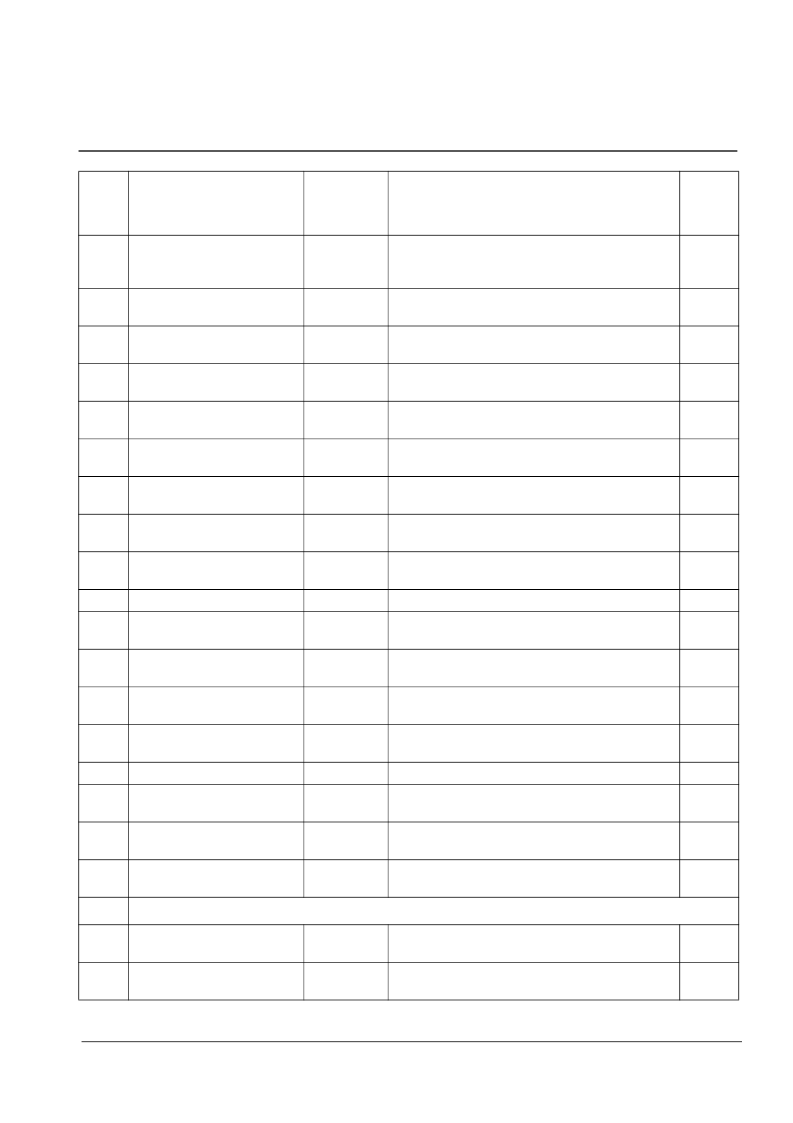
p0_enable
8F
Control register to enable p0_clk0, p0_clk1,
p0_fp0, p0_fp1, the P0 synthesizer and select
the source
R/W
37
p0_run
0F
Control register to generate p0_clk0, p0_clk1,
p0_fp0 and p0_fp1
R/W
38
p0_freq_0
00
Control register for the [7:0] bits of the N of
N*8k clk0
R/W
39
p0_freq_1
01
Control register for the [13:8] bits of the N of
N*8k clk0
R/W
3A
p0_clk0_offset90
00
Control register for the p0_clk0 phase position
coarse tuning
R/W
3B
p0_clk1_div
3E
Control register for the p0_clk1 frequency
selection
R/W
3C
p0_clk1_offset90
00
Control register for the p0_clk1 phase position
coarse tuning
R/W
3D
p0_offset_fine
00
Control register for the output/output phase
alignment fine tuning for p0 path
R/W
3E
p0_fp0_freq
05
Control register to select the p0_fp0 frame
pulse frequency
R/W
3F
p0_fp0_type
83
Control register to select fp0 type
R/W
40
p0_fp0_offset_0
00
Bits [7:0] of the programmable frame pulse
phase offset in multiples of 1/262.14 MHz
R/W
41
p0_fp0_offset_1
00
Bits [15:8] of the programmable frame pulse
phase offset in multiples of 1/262.14 MHz
R/W
42
p0_fp0_offset_2
00
Bits [21:16] of the programmable frame pulse
phase offset in multiples of 8 kHz cycles
R/W
43
p0_fp1_freq
05
Control register to select p0_fp1 frame pulse
frequency
R/W
44
p0_fp1_type
11
Control register to select fp1 type
R/W
45
p0_fp1_offset_0
00
Bits [7:0] of the programmable frame pulse
phase offset in multiples of 1/262.144 MHz
R/W
46
p0_fp1_offset_1
00
Bits [15:8] of the programmable frame pulse
phase offset in multiples of 1/262.144 MHz
R/W
47
p0_fp1_offset_2
00
Bits [21:16] of the programmable frame pulse
phase offset in multiples of 8 kHz cycles
R/W
P1 Configuration Registers
48
p1_enable
83
Control register to enable p1_clk0, p1_clk1, the
P1 synthesizer and select the source
R/W
49
p1_run
03
Control register to generate enable/disable
p1_clk0 and p1_clk1
R/W
Addr
(Hex)
Register
Name
Reset
Value
(Hex)
Description
Type
Table 5 - Register Map (continued)
相關PDF資料 |
PDF描述 |
|---|---|
| ZL30119GGG2 | SONET/SDH OC-48/OC-192 Line Card Synchronizer |
| ZL30120 | SONET/SDH/Ethernet Multi-Rate Line Card Synchronizer |
| ZL30120GGG | SONET/SDH/Ethernet Multi-Rate Line Card Synchronizer |
| ZL30120GGG2 | SONET/SDH/Ethernet Multi-Rate Line Card Synchronizer |
| ZL30121GGG2 | SONET/SDH Low Jitter System Synchronizer |
相關代理商/技術參數 |
參數描述 |
|---|---|
| ZL30119GGG2 | 制造商:Microsemi Corporation 功能描述:LINE CARD SYNCHRONIZER 100CABGA - Trays 制造商:MICROSEMI CONSUMER MEDICAL PRODUCT GROUP 功能描述:IC SONET/SDH SYNCH 100CABGA 制造商:Microsemi Corporation 功能描述:IC SONET/SDH SYNCH 100CABGA |
| ZL30120 | 制造商:ZARLINK 制造商全稱:Zarlink Semiconductor Inc 功能描述:SONET/SDH/Ethernet Multi-Rate Line Card Synchronizer |
| ZL30120GGG | 制造商:Microsemi Corporation 功能描述:T1/E1 SYSTEM SYNCHRONIZER 制造商:Microsemi Corporation 功能描述:LINE CARD SYNCHRONIZER 100CABGA - Trays 制造商:MICROSEMI CONSUMER MEDICAL PRODUCT GROUP 功能描述:IC LINE CARD SYNCH 100CABGA 制造商:Microsemi Corporation 功能描述:IC LINE CARD SYNCH 100CABGA |
| ZL30120GGG2 | 制造商:Microsemi Corporation 功能描述:LINE CARD SYNCHRONIZER 100CABGA - Trays 制造商:MICROSEMI CONSUMER MEDICAL PRODUCT GROUP 功能描述:IC LINE CARD SYNCH 100CABGA 制造商:Microsemi Corporation 功能描述:IC LINE CARD SYNCH 100CABGA |
| ZL30121 | 制造商:ZARLINK 制造商全稱:Zarlink Semiconductor Inc 功能描述:SONET/SDH Low Jitter System Synchronizer |
發(fā)布緊急采購,3分鐘左右您將得到回復。