- 您現(xiàn)在的位置:買賣IC網(wǎng) > PDF目錄371396 > 24FC128 (Microchip Technology Inc.) The CAT24FC02 is a 2-kb Serial CMOS EEPROM internally organized as 256 words of 8 bits each PDF資料下載
參數(shù)資料
| 型號(hào): | 24FC128 |
| 廠商: | Microchip Technology Inc. |
| 元件分類: | EEPROM |
| 英文描述: | The CAT24FC02 is a 2-kb Serial CMOS EEPROM internally organized as 256 words of 8 bits each |
| 中文描述: | 該CAT24FC02是一個(gè)2 KB的EEPROM的國(guó)內(nèi)256個(gè)8位每字舉辦的串行CMOS |
| 文件頁(yè)數(shù): | 1/26頁(yè) |
| 文件大?。?/td> | 450K |
| 代理商: | 24FC128 |
當(dāng)前第1頁(yè)第2頁(yè)第3頁(yè)第4頁(yè)第5頁(yè)第6頁(yè)第7頁(yè)第8頁(yè)第9頁(yè)第10頁(yè)第11頁(yè)第12頁(yè)第13頁(yè)第14頁(yè)第15頁(yè)第16頁(yè)第17頁(yè)第18頁(yè)第19頁(yè)第20頁(yè)第21頁(yè)第22頁(yè)第23頁(yè)第24頁(yè)第25頁(yè)第26頁(yè)

2004 Microchip Technology Inc.
DS21191M-page 1
24AA128/24LC128/24FC128
128K I
2
C
CMOS Serial EEPROM
Device Selection Table
Features
Low-power CMOS technology:
- Maximum write current 3 mA at 5.5V
- Maximum read current 400
μ
A at 5.5V
- Standby current 100 nA typical at 5.5V
2-wire serial interface bus, I
2
C compatible
Cascadable for up to eight devices
Self-timed erase/write cycle
64-byte Page Write mode available
5 ms max write cycle time
Hardware write-protect for entire array
Output slope control to eliminate ground bounce
Schmitt Trigger inputs for noise suppression
1,000,000 erase/write cycles
Electrostatic discharge protection > 4000V
Data retention > 200 years
8-pin PDIP, SOIC, TSSOP, MSOP and DFN
packages, 14-lead TSSOP package
Standard and Pb-free finishes available
Temperature ranges:
- Industrial (I):
-40
°
C to +85
°
C
- Automotive (E):
-40
°
C to +125
°
C
Description
The Microchip Technology Inc. 24AA128/24LC128/
24FC128 (24XX128*) is a 16K x 8 (128 Kbit) Serial
Electrically Erasable PROM (EEPROM), capable of
operation across a broad voltage range (1.8V to 5.5V).
It has been developed for advanced, low-power
applications such as personal communications or data
acquisition. This device also has a page write capabil-
ity of up to 64 bytes of data. This device is capable of
both random and sequential reads up to the 128K
boundary. Functional address lines allow up to eight
devices on the same bus, for up to 1 Mbit address
space. This device is available in the standard 8-pin
plastic DIP, SOIC (150 and 208 mil), TSSOP, MSOP,
DFN and 14-lead TSSOP packages.
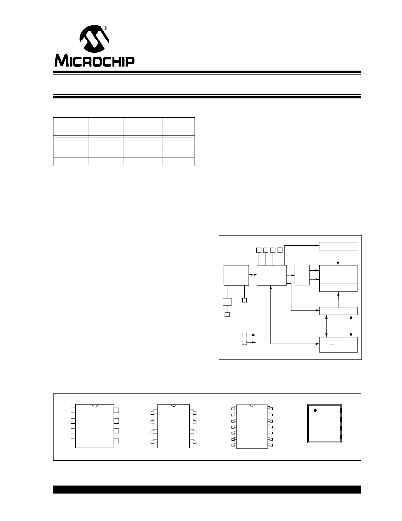
Block Diagram
Package Types
*24XX128 is used in this document as a generic part number for the 24AA128/24LC128/24FC128 devices.
Part
Number
V
CC
Range
Max. Clock
Frequency
Temp.
Ranges
24AA128
1.8-5.5V
400 kHz
(1)
I
24LC128
24FC128
Note 1:
2.5-5.5V
1.8-5.5V
100 kHz for V
CC
< 2.5V.
400 kHz for V
CC
< 2.5V.
400 kHz
1 MHz
(2)
I, E
I
2:
HV Generator
EEPROM
Array
Page Latches
YDEC
XDEC
Sense Amp.
R/W Control
M
emory
C
ontrol
L
ogic
I/O
C
ontrol
L
ogic
I/O
A0 A1 A2
SDA
SCL
V
CC
V
SS
WP
A0
A1
A2
V
SS
V
CC
WP
SCL
SDA
1
2
3
4
8
7
6
5
2
PDIP/SOIC
TSSOP/MSOP *
A0
A1
A2
V
SS
1
2
3
4
8
7
6
5
V
CC
WP
SCL
SDA
TSSOP
2
DFN
A0
A1
A2
V
SS
WP
SCL
SDA
2
5
6
7
8
4
3
2
1
V
CC
NC
NC
NC
A0
A1
A2
V
SS
NC
NC
NC
V
CC
WP
SCL
SDA
2
1
2
3
4
5
6
7
14
13
12
11
10
9
8
Note: *
Pins A0 and A1 are no-connects for the MSOP package only.
相關(guān)PDF資料 |
PDF描述 |
|---|---|
| 24FC256 | 24AA256/LC256/FC256 Datasheet |
| 24FC32 | 32K 5.0V 1 MHz I 2 C Smart Serial EEPROM |
| 24FC32-IP | 32K 5.0V 1 MHz I 2 C Smart Serial EEPROM |
| 24FC32-ISM | 32K 5.0V 1 MHz I 2 C Smart Serial EEPROM |
| 24FC32-P | 32K 5.0V 1 MHz I 2 C Smart Serial EEPROM |
相關(guān)代理商/技術(shù)參數(shù) |
參數(shù)描述 |
|---|---|
| 24FC128-E/CS15K | 制造商:MICROCHIP 制造商全稱:Microchip Technology 功能描述:128K I2Ca?¢ CMOS Serial EEPROM |
| 24FC128-E/MC | 制造商:MICROCHIP 制造商全稱:Microchip Technology 功能描述:128K I2C CMOS Serial EEPROM |
| 24FC128E/MF | 制造商:未知廠家 制造商全稱:未知廠家 功能描述:EEPROM |
| 24FC128-E/MF | 制造商:MICROCHIP 制造商全稱:Microchip Technology 功能描述:128K I2C CMOS Serial EEPROM |
| 24FC128-E/MNY | 制造商:MICROCHIP 制造商全稱:Microchip Technology 功能描述:128K I2Ca?¢ CMOS Serial EEPROM |
發(fā)布緊急采購(gòu),3分鐘左右您將得到回復(fù)。