- 您現(xiàn)在的位置:買賣IC網(wǎng) > PDF目錄372997 > 2N4119A (CALOGIC LLC) N-Channel JFET General Purpose Amplifier PDF資料下載
參數(shù)資料
| 型號(hào): | 2N4119A |
| 廠商: | CALOGIC LLC |
| 元件分類: | 小信號(hào)晶體管 |
| 英文描述: | N-Channel JFET General Purpose Amplifier |
| 中文描述: | N-CHANNEL, Si, SMALL SIGNAL, JFET, TO-72 |
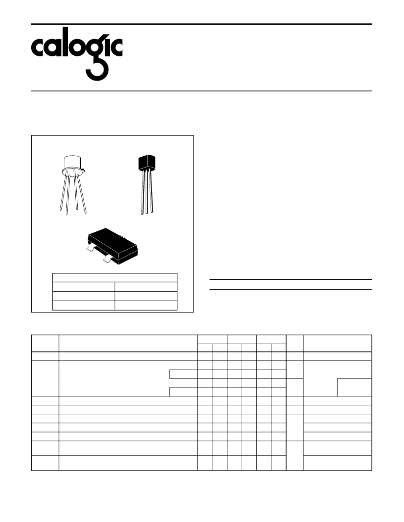
| 封裝: | HERMETIC SEALED PACKAGE-4 |
| 文件頁(yè)數(shù): | 1/1頁(yè) |
| 文件大小: | 21K |
| 代理商: | 2N4119A |
N-Channel JFET
General Purpose Ampifier
2N4117 – 2N4119 /2N4117A – 2N4119A
PN4117 – PN4119 /PN4117A – PN4119A /SST4117 – SST4119
FEATURES
Low Leakage
Low Capacitance
ABSOLUTE MAXIMUM RATINGS
(T
A
= 25
o
C unless otherwise noted)
Gate-Source or Gate-Drain Voltage . . . . . . . . . . . . . . . . -40V
Gate Current . . . . . . . . . . . . . . . . . . . . . . . . . . . . . . . . . 50mA
Storage Temperature Range . . . . . . . . . . . . . -65
o
C to +200
o
C
Operating Temperature Range . . . . . . . . . . . -55
o
C to +175
o
C
Lead Temperature (Soldering, 10sec). . . . . . . . . . . . . +300
o
C
Power Dissipation . . . . . . . . . . . . . . . . . . . . . . . . . . . . 300mW
Derate above 25
o
C . . . . . . . . . . . . . . . . . . . . . . . 2.0mW/
o
C
NOTE:
Stresses above those listed under "Absolute Maximum
Ratings" may cause permanent damage to the device. These are
stress ratings only and functional operation of the device at these or
any other conditions above those indicated in the operational sections
of the specifications is not implied. Exposure to absolute maximum
rating conditions for extended periods may affect device reliability.
ORDERING INFORMATION
Part
2N4117-19/A Hermetic TO-72
PN4117-19/A Plastic TO-92
SST4117-19
Plastic SOT-23
X2N4117-19/A Sorted Chips in Carriers
Package
Temperature Range
-55
o
C to +175
o
C
-55
o
C to +135
o
C
-55
o
C to +135
o
C
-55
o
C to +175
o
C
C ORPORATION
PIN CONFIGURATION
TO-72
G
D
C
S
ELECTRICAL CHARACTERISTICS
(T
A
= 25
o
C unless otherwise specified)
SYMBOL
PARAMETER
4117/A
MIN MAX MIN MAX MIN MAX
-40
-40
4118/A
4119/A
UNITS
TEST CONDITIONS
BV
GSS
Gate-Source Breakdown Voltage
-40
V
I
G
= -1
μ
A, V
DS
= 0
I
GSS
Gate Reverse Current
-10
-10
-10
pA
A devices
-1
-1
-1
V
GS
= -20V, V
DS
= 0
-25
-25
-25
nA
T
A
= +150
o
C
A devices
-2.5
-2.5
-2.5
V
GS(off)
Gate-Source Pinch-Off Voltage
-0.6
-1.8
-1
-3
-2
-6
V
V
DS
= 10V, I
D
= 1nA
I
DSS
g
fs
g
fs
Drain Current at Zero Gate Voltage (Note 1)
0.02 0.09 0.08 0.24 0.20 0.60
mA
V
DS
= 10V, V
GS
= 0
V
DS
= 10V, f = 1kHz
V
GS
= 0, f = 30MHz
Common-Source Forward Transconductance (Note 1)
70
210
80
250
100
330
μ
S
Common-Source Forward Transconductance (Note 2)
60
70
90
g
os
Common-Source Output Conductance
3
5
10
V
DS
= 10V, V
GS
= 0, f = 1kHz
V
DS
= 10V, V
GS
= 0,
f = 1MHz
V
DS
= 10V, V
GS
= 0,
f = 1MHz
C
iss
Common-Source Input Capacitance (Note 2)
3
3
3
pF
C
rss
Common-Source Reverse Transfer Capacitance (Note 2)
1.5
1.5
1.5
NOTES: 1.
Pulse test: Pulse duration of 2ms used during test.
2.
For design reference only, not 100% tested.
D
S
G
TO-92
SOT-23
G
S
D
PRODUCT MARKING (SOT-23)
SST4117
T17
SST4118
T18
SST4119
T19
5007
相關(guān)PDF資料 |
PDF描述 |
|---|---|
| 2N4119 | ULTRA-HIGH INPUT IMPEDANCE N-CHANNEL JFET |
| 2N4119A | ULTRA-HIGH INPUT IMPEDANCE N-CHANNEL JFET |
| 2N4403 | Si-Epitaxial PlanarTransistors |
| 2N5021 | P-Channel Silicon Junction Field-Effect Transistor |
| 2N5064 | SCR |
相關(guān)代理商/技術(shù)參數(shù) |
參數(shù)描述 |
|---|---|
| 2N4119A_TO-71 | 制造商:MICROSS 制造商全稱:MICROSS 功能描述:an Ultra-High Input Impedance N-Channel JFET |
| 2N4119A-2 | 制造商:Vishay Siliconix 功能描述:SS SOT23 GP XSTR NPN 65V - Bulk |
| 2N4119A-E3 | 功能描述:JFET 40V 0.2mA RoHS:否 制造商:ON Semiconductor 晶體管極性:N-Channel 漏極電流(Vgs=0 時(shí)的 Idss):50 mA 漏源電壓 VDS:15 V 閘/源擊穿電壓: 漏極連續(xù)電流:50 mA 配置: 安裝風(fēng)格: 封裝 / 箱體:SC-59 封裝:Reel |
| 2N412 | 制造商:未知廠家 制造商全稱:未知廠家 功能描述:TRANSISTOR | BJT | PNP | 15MA I(C) | TO-1 |
| 2N4120 | 制造商:未知廠家 制造商全稱:未知廠家 功能描述:TRANSISTOR | MOSFET | P-CHANNEL | 30V V(BR)DSS | 20MA I(D) | TO-72 |
發(fā)布緊急采購(gòu),3分鐘左右您將得到回復(fù)。