- 您現(xiàn)在的位置:買賣IC網(wǎng) > PDF目錄67320 > 5962-005300HXX (ANALOG DEVICES INC) DUAL 1-CH 12-BIT PROPRIETARY METHOD ADC, PARALLEL ACCESS, CQFP68 PDF資料下載
參數(shù)資料
| 型號(hào): | 5962-005300HXX |
| 廠商: | ANALOG DEVICES INC |
| 元件分類: | ADC |
| 英文描述: | DUAL 1-CH 12-BIT PROPRIETARY METHOD ADC, PARALLEL ACCESS, CQFP68 |
| 封裝: | CERAMIC, LCC-68 |
| 文件頁(yè)數(shù): | 2/20頁(yè) |
| 文件大小: | 3346K |
| 代理商: | 5962-005300HXX |
第1頁(yè)當(dāng)前第2頁(yè)第3頁(yè)第4頁(yè)第5頁(yè)第6頁(yè)第7頁(yè)第8頁(yè)第9頁(yè)第10頁(yè)第11頁(yè)第12頁(yè)第13頁(yè)第14頁(yè)第15頁(yè)第16頁(yè)第17頁(yè)第18頁(yè)第19頁(yè)第20頁(yè)
This information applies to a product which is in development. Specifications are subject to change without notice. Contact factory for most
recent information. Analog Devices Sensitive Material - not to be reproduced or distributed without permission.
Rev. Pr E
10
THEORY OF OPERATION
The AD13280 is a high-dynamic range 12-bit, 80MHz pipline delay (3
pipelines) analog-to-digital converter. The custom analog input section
provides input ranges of 1 and 2 vp-p and input impedance configura-
tions of 50, 100 and 200 ohms.
The AD13280 employs four monolithic ADI components per channel
(AD8037, AD8138, AD8031, and a custom ADC IC), along with
multiple passive resistor networks and decoupling capacitors to fully
integrate a complete 12-bit analog-to-digital converter.
In the single ended input configuration the input signal is passed
through a precision laser trimmed resistor divider allowing the user to
externally select operation with a full scale signal of ±0.5V, or ±1.0V by
choosing the proper input terminal for the application. The result of the
resistor divider is to apply a full-scale input approximately 0.4V to the
non-inverting input of the internal AD8037 amplifier.
The AD13280 analog input includes an AD8037 amplifier featuring an
innovative architecture that maximizes the dynamic range capability on
the amplifiers inputs and outputs. The AD8037 amplifier provides a
high input impedance and gain for driving the AD8138 in a single-
ended to differential amplifier configuration. The AD8138 has a -3dB
bandwidth at 300MHz and delivers a differential signal with the lowest
harmonic distortion available in a differential amplifier. The AD8138
differential outputs help balance the differential inputs to the custom
ADC maximizing the performance of the device.
The AD8031 provides the buffer for the internal reference analog-to-
digital comverter. The internal reference voltage of the custom ADC is
designed to track the offsets and drifts and is used to ensure matching
over an extended temperature range of operation. The reference voltage
is connected to the output common mode input on the AD8138. This
reference voltage sets the output common mode on the AD8138 at 2.4V,
which is the mid-supply level for the ADC.
The custom ADC has complementary analog input pins, AIN and AIN.
Each analog input is centered at 2.4V and should swing ±0.55V around
this reference. Since AIN and AIN are 180 degrees out of phase, the
differential analog input signal is 2.2V peak-to-peak. Both analog
inputs are buffered prior to the first track-and-hold.
The custom ADC digital outputs drive 100 ohm series resistors (Figure
5.) The result is a 12-bit parallel digital CMOS-compatible word, coded
as two’s complement.
USING THE SINGLE-ENDED INPUT
The AD13280 has been designed with the user’s ease of operation in
mind. Multiple input configurations have been included on board to
allow the user a choice of input signal levels and input impedance. The
standard inputs are ±0.5V and ±1.0V. The user can select the input
impedance of the AD13280 on any input by using the other inputs as
alternate locations for the GND. The following chart summarizes the
impedance options available at each input location.
AMP-IN-X-1 = 100
when AMP-IN-X-2 open
AMP-IN-X-1 = 50
when AMP-IN-X-2 is shorted to GND
AMP-IN-X-2 = 200
when AMP-IN-X-1 open
Each channel has two analog inputs AMP-IN-A-1 and AMP-IN-A-2 or
AMP-IN-B-1 and AMP-IN-B-2. Use AMP-IN-A-1 or AMP-IN-B-1
when an input of ±.5V fullscale is desired. Use AMP-IN-A-2 or AMP-
IN-B-2 when ±1V fullscale is desired. Each channel has an AMP-OUT
which must be tied to either a non-inverting or inverting input of a
differential amplifier with the remaining input grounded. For example,
Side A, AMP-OUT-A (Pin 6) must be tied to A+IN (Pin 5) with A-IN
(Pin 5) tied to ground for non-inverting operation or AMP-OUT-A (pin
6) tied to A-IN (Pin 4) with A+IN (Pin 5) tied to ground for inverting
operation.
AD13280
USING THE DIFFERENTIAL INPUT
Each channel of the AD13280 was designed with two optional
differential inputs, A+IN, A-IN and B+IN, B-IN. The inputs provide
system designers with the ability to bypass the AD8037 amplifier and
drive the AD8138 directly. The AD8138 differential ADC driver can be
deployed in either a single-ended or differential input configuration.
The differential analog inputs have a nominal input impedance of 620
ohms and nominal full-scale input range of 1.2Vp-p. The AD8138
amplifier drives a differential filter and the custom analog-to-digital
converter. The differential input configuration provides the lowest
even-order harmonics and signal-to-noise (SNR) performance
improvement of up to 3dB (SNR = 73dBFS). Exceptional care was
taken in the layout of the differential input signal paths. The differential
input transmission line characteristics are matched and balanced. Equal
attention to system level signal paths must be provided in order to
realize significant performance improvements.
APPLYING THE AD13280
Encoding the AD13280
The AD13280 encode signal must be a high quality, extremely low
phase noise source, to prevent degradation of performance. Maintaining
12-bit accuracy at 80MSPS places a premium on encode clock phase
noise. SNR performance can easily degrade 3 dB to 4 dB with 37MHz
input signals when using a high-jitter clock source. See Analog
Devices’ Application Note AN-501, “Aperture Uncertainty and ADC
System Performance” for complete details. For optimum performance,
the AD13280 must be clocked differentially. The encode signal is
usually ac-coupled into the ENCODE and ENCODE pins via a
transformer or capacitors. These pins are biased internally and require
no additional bias.
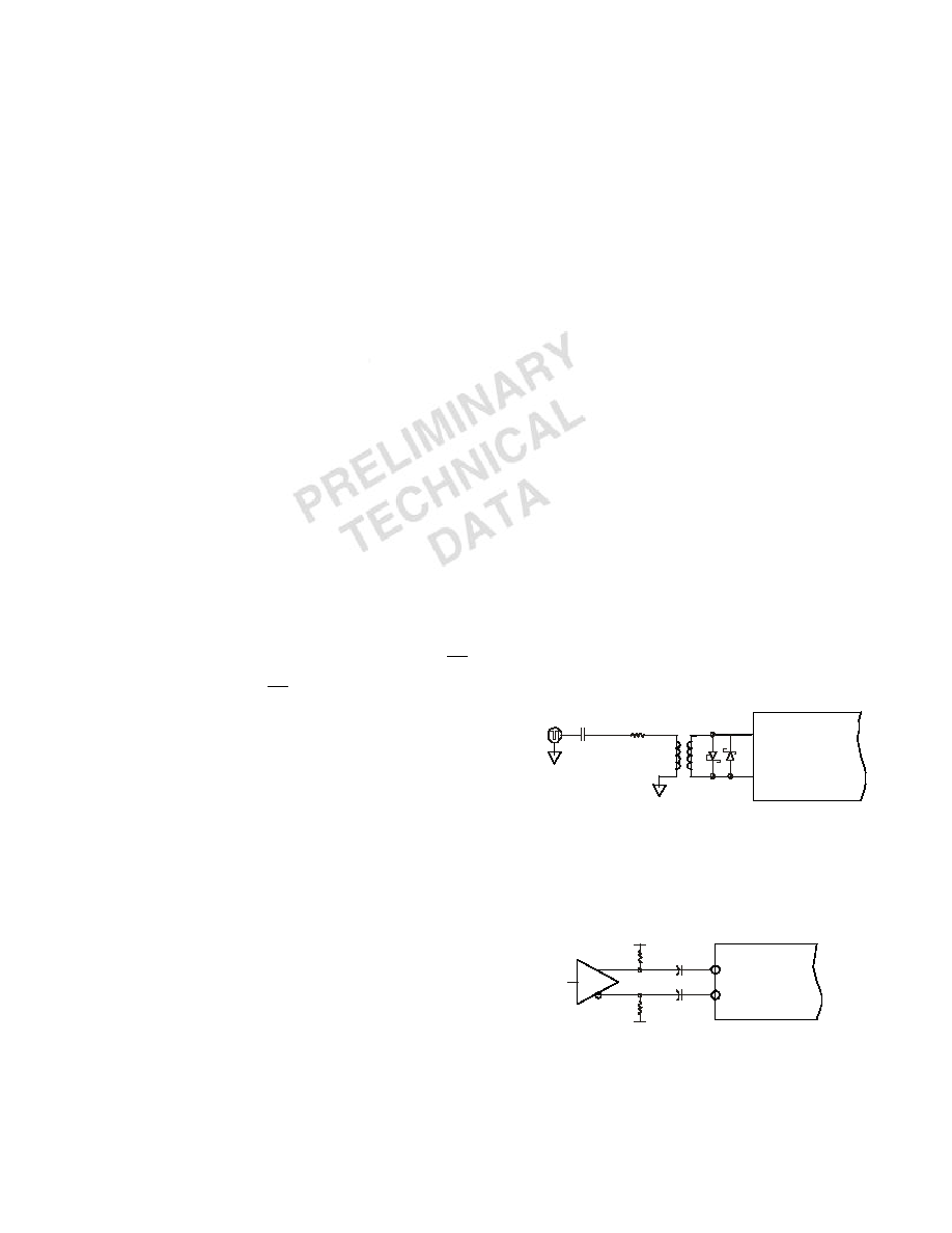
Shown below is one preferred method for clocking the AD13280. The
clock source (low jitter) is converted from single-ended to differential
using an RF transformer. The back-to-back Schottky diodes across the
transformer secondary limit clock excursions into the AD13280 to
approximately 0.8 V p-p differential. This helps prevent the large
voltage swings of the clock from feeding through to the other portions
of the AD13280, and limits the noise presented to the ENCODE inputs.
A crystal clock oscillator can also be used to drive the RF transformer if
an appropriate limited resistor (typically 100
) is placed in the series
with the primary.
Figure 6: Crystal Clock Oscillator - Differential Encode
If a low jitter ECL/PECL clock is available, another option is to ac-
couple a differential ECL/PECL signal to the encode input pins as
shown below. A device that offers excellent jitter performance is the
MC100LVEL16 (or same family) from Motorola.
Figure 7. Differential ECL for Encode
ENCO DE
AD13280
T1-4T
HSMS2812
DIODES
CLOCK
SOURCE
0.1mF
100V
ENCODE
AD13280
0.1mF
0.1m F
VT
ECL/
PEC L
相關(guān)PDF資料 |
PDF描述 |
|---|---|
| 5962-0150601HXX | DUAL 1-CH 14-BIT PROPRIETARY METHOD ADC, PARALLEL ACCESS, CQFP68 |
| 5962-0251002HXC | 1-OUTPUT 8 W DC-DC REG PWR SUPPLY MODULE |
| 5962-9213902HZC | 1-OUTPUT 12 W DC-DC REG PWR SUPPLY MODULE |
| 5962-9555902HXC | 2-OUTPUT 12 W DC-DC REG PWR SUPPLY MODULE |
| 5962-9214402HXC | 2-OUTPUT 15 W DC-DC REG PWR SUPPLY MODULE |
相關(guān)代理商/技術(shù)參數(shù) |
參數(shù)描述 |
|---|---|
| 5962005304899 | 制造商: 功能描述: 制造商:undefined 功能描述: |
| 5962005308115 | 制造商: 功能描述: 制造商:undefined 功能描述: |
| 5962005345643 | 制造商: 功能描述: 制造商:undefined 功能描述: |
| 5962-0053901QYA | 制造商:TI 制造商全稱:Texas Instruments 功能描述:DIGITAL SIGNAL PROCESSOR |
| 5962-0053901QYC | 制造商:TI 制造商全稱:Texas Instruments 功能描述:DIGITAL SIGNAL PROCESSOR |
發(fā)布緊急采購(gòu),3分鐘左右您將得到回復(fù)。